
51 - 60 of 159
single crystal gallium nitride wafer
Selling leads
|
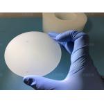
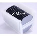
8inch Dia200mm C-Plane Al2O3 99.999% Sapphire Single Crystal Wafer Carrier Substrate 1sp 2sp *, *::before, *::after {box-sizing: border-box; } * ...
2025-08-01 00:08:35
|
|
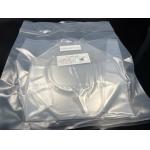
...wafer for LeD, semiconducting Gallium Nitride Wafer for ld, GaN template, mocvd GaN Wafer,Free-standing GaN Substrates by Customized size, small ...
2025-05-06 20:44:15
|
|
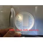
...LED, mocvd Gallium Nitride wafer 10x10mm,5x5mm, 10x5mm GaN wafer,Non-Polar Freestanding GaN Substrates(a-plane and m-plane) 4inch 2inch free...
2025-05-06 20:44:19
|
|
4inch diameter 100mm Lithium niobate LiNbO3 substrate wafer, LN wafer for saw and optical,SAW Grade LiNbO3 Crystal ingot Description: Lithium niobate ...
2025-05-06 20:44:35
|
|
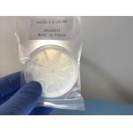
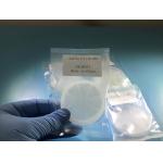
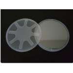
2inch /3inch 4inch /5inch C-axis/ a-axis/ r-axis/ m-axis 6"/6inch dia150mm C-plane Sapphire SSP/DSP wafers with 650um/1000um Thickness TTV
2025-05-06 20:38:48
|
|
...Nitride Template on 430um sapphire/ 350um Sic substrates AlN Wafer Characteristic III-Nitride(GaN,AlN,InN) 2inch AlN template on sapphire or sic ...
2025-05-06 20:44:29
|
|
Ni Substrate single crystal cubic structure a=3.25A purity 99.99% density 8.91 Ni Substrate's abstract Nickel (Ni) substrates, particularly in the ...
2025-05-06 20:45:48
|
|
diameter 150mm 8inch 4inch 6inch Silicon-based AlN templates 500nm AlN film on silicon substrate Applications of AlN template Silicon-based semiconduc...
2025-05-06 20:44:41
|
|
Product Description: Our InP (Indium Phosphide) wafers are renowned for their low defect density and high performance, widely used in optoelectronics ...
2025-05-06 20:44:24
|
|
...Gallium arsenide GaAs Wafer Product Description (GaAs) Gallium Arsenide Wafers PWAM Develops and manufactures compound semiconductor substrates...
2025-05-06 20:44:31
|