
101 - 110 of 159
single crystal gallium nitride wafer
Selling leads
|
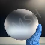
...Wafer Si Substrate 111 P Type N Type for Micro-electromechanical systems (MEMS) Or Power semiconductor devices Or Optical components and sensors ...
2025-05-06 20:45:50
|
|
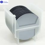
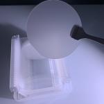
High Purity 4 6 8-inch conductive semi insulation SiC single crystal wafer/8 Inches (200mm) Monocrystalline Double Side Polished SiC Wafer/Silicon ...
2025-05-06 20:41:06
|
|
...crystals crystal substrate TeO2 wafer TeO2 Crystal & Q Switch TeO2 is an excellent ascousto-optic (AO) crystal with high AO figure of merit, ...
2025-05-06 20:40:28
|
|
..., optoelectronic devices, semiconductor devices, and other fields. The high light transmittance and high hardness of sapphire wafers make them ...
2025-08-03 00:08:11
|
|
...crystal. It belongs to the cubic crystal system. Nd∶GGG doped with Nd is an excellent laser crystal, which can obtain pulsed laser output at room ...
2025-05-06 20:40:33
|
|
...Miscut A 4 Degree Sapphire Wafers Thickness 0.175mm/0.3mm/0.4mm/0.5mm Dsp 2 Inch C Plane Polished Sapphire Wafers Crystal Substrates The specificat...
2025-08-03 00:08:11
|
|
... growth 430um SSP DSP About synthetic sapphire crystal Due to the less mismatched lattice and stable chemical and physical properties, sapphire...
2025-08-03 00:08:11
|
|
... and low propagation loss, which can be used to fabricate SAW devices with up to 50% bandwidth. The acoustic surface wave properties of lithium ...
2025-05-06 20:45:00
|
|
... conductivity properties, which can be precisely modified through doping with elements like phosphorus or boron, make them ideal for fabricating ...
2025-05-06 20:45:58
|
|
...strontium aluminate (LSAT)crystals crystal substrate wafer/LSAT (LaAlO3)0.3 (Sr2AlTaO8)0.7 Single Crystal Monocrystal Substrate Product Name...
2025-05-06 20:40:29
|