
111 - 120 of 150
semiconductor silicon on sapphire wafers
Selling leads
|
...Wafer Semiconductor Substrate For Epitaxial Growth VGF 2inch 4inch 6inch n-type prime grade GaAs wafer for epitaxial growth Gallium arsenide can be ...
2025-05-06 20:45:00
|
|
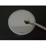
...Wafer Si Substrate 111 P Type N Type for Micro-electromechanical systems (MEMS) Or Power semiconductor devices Or Optical components and sensors ...
2025-05-06 20:45:50
|
|
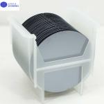
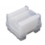
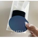
...wafer carrier container cassette box for wafer shipment factory price 6" Diameter Single Wafer Carrier Box Wafer Box Customized Processing Square ...
2025-05-06 20:47:35
|
|
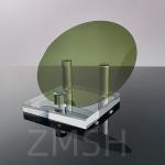
AlN on Diamond template wafers AlN epitaxial films on Diamond substrate AlN on Sapphire /AlN-on-SiC/ AlN-ON Silicon Welcome to Know AlN Template on ...
2025-05-06 20:44:22
|
|
...second-generation semiconductor materials represented by silicon (Si) and gallium arsenide (GaAs) has propelled the swift advancement of microelect...
2025-05-06 20:41:29
|
|
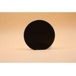
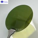
... optical lens for intermediate infrared laser Nonlinear optical and quantum optics lens About Silicon Carbide (SiC)Crystal Silicon carbide (SiC), ...
2025-05-06 20:40:53
|

|
...Sapphire Tube Advantages Our Sapphire tubes provide a number of advantages for semiconductor processing applications, as compared to quartz, ...
2025-07-30 00:08:00
|
|
Silicon Carbide (SiC) Optical Lens – Infrared & Laser Applications Product Overview of Silicon Carbide (SiC) Optical Lens Silicon Carbide (SiC) lenses ...
2025-06-24 07:30:26
|
|
SiC Epitaxial Wafer Overview 4-inch (100 mm) SiC Epitaxial Wafers continue to play a vital role in the semiconductor market, serving as a highly ...
2025-07-10 18:23:23
|
|
SiO2 wafer Thermal Oxide Laver Thickness 20um+5% MEMS Optical Communication System Product Description: The SIO2 silicon dioxide wafer serves as a ...
2025-05-06 20:45:05
|