
31 - 40 of 42
rf devices gallium nitride wafer
Selling leads
|
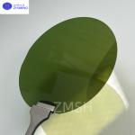
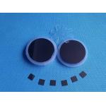
...RF device manufacturers worldwide. The 4” wafer size strikes an excellent balance between performance, availability, and cost-effectiveness—making ...
2025-07-10 18:23:23
|
|
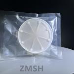
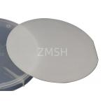
...Wafer 4H/6H-P Silicon Carbide Substrate DSP (111) Semiconductor RF Microwave LED Lasers Description of SiC Wafer: The 6-inch P-Type Silicon Carbide ...
2025-05-06 20:41:42
|
|
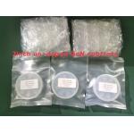
... wafer Applications of AlN template Silicon-based semiconductor technology has reached its limits and could not satisfy the requirements of future ...
2025-05-06 20:44:39
|
|
10x10mmt Terbium gallium garnet (TGG)crystals substrate wafer for laser device Product Type: Yttrium aluminum garnet (YAG) is an isotropic crystal ...
2025-07-23 00:09:03
|
|
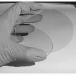
2-4inch Gallium antimonide GaSb Substrate Single Crystal Monocrystal for Semiconductor InAsSb/In-AsPSb, InNAsSb and other heterojunction materials can ...
2025-05-06 20:44:36
|
|
Abstract The 4-H Semi-Insulating SiC substrate is a high-performance semiconductor material with a wide range of applications. It derives its name ...
2025-07-23 00:09:03
|
|
...Wafer Flat or PPS Sapphire MOCVD DSP SSP Description of GaN-on-Sapphire Blue/Green LED Wafer: GaN on Sapphire (GaN/Sapphire) wafers refers to a ...
2025-05-06 20:44:26
|
|
2inch 4inch 4" 2'' Sapphire based GaN templates GaN film on the sapphire substrate GaN-On-Sapphire GaN wafers GaN substrates GaN windows Properties of ...
2025-05-06 20:44:20
|
|
...Sapphire The growth of superconducting compounds / Gallium Nitride Infrared detectors Hybrid microelectronics Polishing carriers Hostile environmen...
2025-05-06 20:37:41
|

|
... application Application Sapphire wafer and substrate applications include: Microelectronic IC applications SOS Silicon-on-Sapphire The growth of ...
2025-05-06 20:37:41
|