
1 - 8 of 8
optical communication system sio2 wafer
Selling leads
|
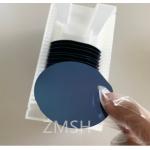
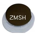
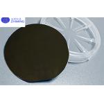
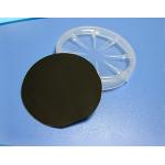
SiO2 wafer Thermal Oxide Laver Thickness 20um+5% MEMS Optical Communication System Product Description: The SIO2 silicon dioxide wafer serves as a ...
2025-05-06 20:45:05
|

|
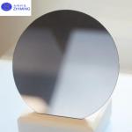
...SiO2) On Silicon Wafers For Optical Communication System Generally, the oxide layer thickness of silicon wafers is mainly concentrated below 3um, ...
2025-08-01 00:08:35
|
|
...wafers, renowned for their exceptional electronic and optoelectronic properties, have found extensive applications in communications, optics, and ...
2025-05-06 20:44:23
|
|
...Wafers Thickness 0.5mm High Transmittance UV Quartz Glass Sheet 0.2mm--- 1.0mm thickness LED Back Light quartz/borofloat Glass Wafer Polished ...
2025-05-06 20:39:24
|
|
... wafer for FP laser diode N-InP substrate FP Epiwafer's Overview Our N-InP Substrate FP Epiwafer is a high-performance epitaxial wafer designed for ...
2025-05-06 20:45:35
|
|
...Wafer Indium phosphide (InP) is an important compound semiconductor material with the advantages of high electronic limit drift speed, good ...
2025-05-06 20:44:34
|
|
...critical components used in high-speed optical communication systems, particularly for 2.5 Gbps to 25 Gbps DFB (Distributed Feedback) laser diodes. ...
2025-05-06 20:45:38
|
|
... optical applications, particularly for Gigabit Ethernet and digital data link communication. Built on a 6-inch wafer, it features a high ...
2025-05-06 20:45:39
|