
101 - 110 of 134
m plane sapphire substrate
Selling leads
|
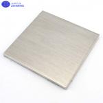
... mm, and 20x20x0.5 mm, are key components in advanced materials research and electronics. These nickel substrates are oriented along crystallograph...
2025-05-06 20:45:48
|
|
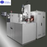
Sapphire Crystal Growth furnance KY Kyropoulos method 90-400kg for sapphire manufacture KY Sapphire Crystal Growth furnance's abstract This Sapphire ...
2025-05-06 20:43:46
|
|
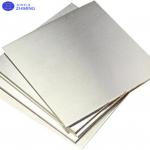
... materials research and applications due to their unique physical properties, such as lightweight and excellent thermal conductivity. These Mg ...
2025-05-06 20:45:46
|
|
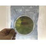
...substrate wafer for laser device Product Type: Terbium gallium garnet (TGG) crystal substrateProduct Description:TGG crystal with a large magneto...
2025-05-06 20:40:28
|
|
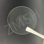
TGV (Through-Glass Via) Glass is an advanced substrate technology that enables vertical electrical interconnections through micro-holes drilled into ...
2025-05-27 17:33:43
|
|
... Substrate Single Crystal Monocrystal for Semiconductor Gallium antimonide (GaSb) is a very important III-V direct bandgap semiconductor material. ...
2025-05-06 20:44:35
|
|
...Sapphire Epi-wafer 1-5um AlN template 8inch 6inch AlGaN/GaN HEMT-on-HR Si Epiwafer GaN-on-Si Epiwafer for Micro-LED for RF application GaN Wafer ...
2025-05-06 20:44:19
|
|
Customzied size/10x10x0.5mmt/2inch/3inch/4inch/6inch 6H-N/4H-SEMI/ 4H-N SIC ingots/High purity 4H-N 4inch 6inch dia 150mm silicon carbide single ...
2025-08-01 00:08:35
|
|
4H-N Testing grade 6inch dia 150mm silicon carbide single crystal (sic) substrates wafers, sic crystal ingots sic semiconductor substrates,Silicon ...
2025-05-06 20:40:37
|
|
AlN on Diamond template wafers AlN epitaxial films on Diamond substrate AlN on Sapphire /AlN-on-SiC/ AlN-ON Silicon Welcome to Know AlN Template on ...
2025-05-06 20:44:22
|