
41 - 50 of 151
high purity single crystal silicon wafer
Selling leads
|
...crystal circle lens,Al2O3 single crystal glass wafer, sapphire lens sapphire optical lens, Al2O3 single crystal glass ,sapphire optical glass ...
2025-05-06 20:37:47
|
|
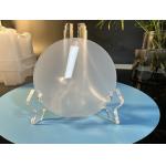
... for 2inch, 4inch, 6inch sapphire substrates and sapphire windows. It is characterized by its extremely low surface roughness (Ra
2025-05-06 20:39:31
|
|
...single crystal wafers Applications of AlN template Silicon-based semiconductor technology has reached its limits and could not satisfy the ...
2025-05-06 20:44:41
|
|
...making them highly desirable for a wide range of applications. In fact, sapphire is one of the hardest and most scratch-resistant materials ...
2025-07-23 00:09:03
|
|
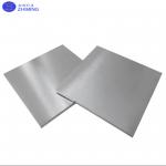
... of electronics and optoelectronics. This study explores aluminum substrates sized at 5×5×1 mm, 10×10×1 mm, and 20×20×0.5 mm, all characterized by ...
2025-05-06 20:45:42
|
|
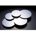
... as the foundation for high-performance semiconductor devices. Crafted with advanced float-zone mono-crystalline silicon technology, this substrate ...
2025-05-06 20:45:11
|
|
...) for sapphire crystal growth is currently used by many companies in China to produce sapphire for the electronics and optics industries. High...
2025-05-06 20:42:09
|
|
...Single Crystal Wafer Indium phosphide (InP) is an important compound semiconductor material with the advantages of high electronic limit drift ...
2025-05-06 20:44:34
|
|
...wafers 3inch 4inch N/P TYPE InP Semiconductor Substrate Wafers Doped S+/ Zn+ /Fe + growth (modified VFG method) is used to pull a single crystal ...
2025-05-06 20:44:36
|
|
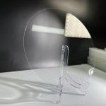
Ultra-thin 2inch sapphire DSP wafers thickness 100um 0.1mm 2inch 100um Ultra Thin sapphire wafers 0.1mm Thickness C-plane DSP Sapphire wafer Why ...
2025-07-23 00:09:03
|