
21 - 30 of 54
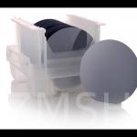
gan wafer thinning machine
Selling leads
|
...) are 3D integrated at the wafer scale. The two wafers are bonded face-to-face using a low-temperature oxide-oxide bonding technique. The Si ...
2025-05-06 20:44:26
|
|
...wafer 1mm thickness for ingot growth Customzied size/2inch/3inch/4inch/6inch 6H-N/4H-SEMI/ 4H-N SIC ingots/High purity 4H-N 4inch 6inch dia 150mm ...
2025-05-06 20:42:04
|
|
...Ready SiC Substrate/Wafers (150mm, 200mm) Silicon Carbide(SiC) wafer N Type 6inch SIC Wafer 4H-N Type production grade sic epitaxial wafers GaN ...
2025-05-06 20:41:08
|
|
...wafer 1mm thickness for ingot growth Customzied size/2inch/3inch/4inch/6inch 6H-N/4H-SEMI/ 4H-N SIC ingots/High purity 4H-N 4inch 6inch dia 150mm ...
2025-05-06 20:40:57
|
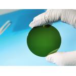
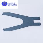
SiC Wafer Hand for Wafer Handling, Cleanroom Compatible, Corrosion Resistant, Customizable Interface
|
... mechanical strength, corrosion resistance, thermal durability, and ultra-clean performance. It is ideal for handling advanced semiconductor ...
2025-05-29 00:09:29
|
|
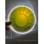
2inch 4inch 4" Sapphire based GaN templates GaN film on sapphire substrate Properties of GaN Chemical properties of GaN 1) At room temperature, GaN is ...
2025-05-06 20:39:23
|
|
... during the range of visible and near IR spectrum.It is widely used for led substrates for GaN Epitaxial growth ;and also as optical window in ...
2025-05-06 20:40:21
|
|
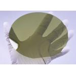
2inch R-axis sapphire wafer for epi-ready test ,sapphire optical windows, R-axis 2inch sapphire epi-ready substrate 1. Description Sapphire is one of ...
2025-05-06 20:44:14
|
|
customzied size MPCVD method GaN&Diamond Heat Sink wafers for Thermal management area According to statistics, the temperature of the working junction ...
2025-05-06 20:44:23
|
|
GaN-on-Si(111) N/P Ttype substrate Epitaxy 4inch 6inch 8inch for LED or Power device GaN-on-Si substrate abstract GaN-on-Si (111) substrates are ...
2025-05-06 20:45:21
|