
11 - 20 of 34
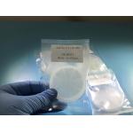
epitaxial hemt gallium nitride wafer
Selling leads

|
... industries, owing to their unique material properties. With a wide bandgap, high electron mobility, and exceptional thermal stability, GaN wafers ...
2025-05-06 20:44:25
|
|
...wafer for LeD,semiconducting Gallium Nitride Wafer for ld,GaN template, mocvd GaN Wafer,Free-standing GaN Substrates by Customized size,small size ...
2025-05-06 20:44:30
|
|
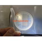
2inch R-axis sapphire wafer for epi-ready test ,sapphire optical windows, R-axis 2inch sapphire epi-ready substrate 1. Description Sapphire is one of ...
2025-05-06 20:44:14
|
|
...wafer for LeD,semiconducting Gallium Nitride Wafer for ld,GaN template, mocvd GaN Wafer,Free-standing GaN Substrates by Customized size,small size ...
2025-05-06 20:44:12
|
|
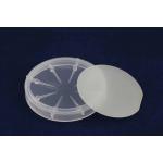
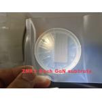
...HEMT-on-HR Si Epiwafer GaN-on-Si Epiwafer for Micro-LED for RF application GaN Wafer Characteristic III-Nitride(GaN,AlN,InN) Gallium Nitride is one ...
2025-05-06 20:44:18
|
|
...Nitride Template on 430um sapphire/ 350um Sic substrates AlN Wafer Characteristic III-Nitride(GaN,AlN,InN) 2inch AlN template on sapphire or sic ...
2025-05-06 20:44:29
|
|
...wafer for LeD,semiconducting Gallium Nitride Wafer for ld,GaN template, mocvd GaN Wafer,Free-standing GaN Substrates by Customized size,small size ...
2025-05-06 20:44:28
|
|
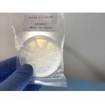
...wafer for LeD, semiconducting Gallium Nitride Wafer for ld, GaN template, mocvd GaN Wafer,Free-standing GaN Substrates by Customized size, small ...
2025-05-06 20:44:15
|
|
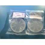
...LED, mocvd Gallium Nitride wafer 10x10mm,5x5mm, 10x5mm GaN wafer,Non-Polar Freestanding GaN Substrates(a-plane and m-plane) 4inch 2inch free...
2025-05-06 20:44:19
|
|
8inch GaN-on-Si Epitaxy Wafer 110 111 110 N-type P-type Customization Semiconductor RF LED Description of GaN-on-Si Wafers: The 8-inch-diameter GaN-on...
2025-05-06 20:44:26
|