
21 - 30 of 34
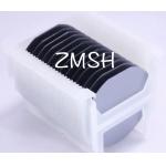
epitaxial hemt gallium nitride wafer
Selling leads
|
AlN on Diamond template wafers AlN epitaxial films on Diamond substrate AlN on Sapphire /AlN-on-SiC/ AlN-ON Silicon Welcome to Know AlN Template on ...
2025-05-06 20:44:22
|
|
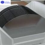
2inch/3inch /4inch /6inch S-C-N Type Si-doped Gallium arsenide GaAs Wafer Product Description (GaAs) Gallium Arsenide Wafers PWAM Develops and ...
2025-05-06 20:44:31
|
|
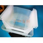
VGF 2 Inch 4Inch N Type P Type GaAs Wafer Semiconductor Substrate For Epitaxial Growth VGF 2inch 4inch 6inch n-type prime grade GaAs wafer for ...
2025-05-06 20:45:00
|
|
Product Description: Our InP (Indium Phosphide) semiconductor wafers, renowned for their exceptional electronic and optoelectronic properties, have ...
2025-05-06 20:44:23
|
|
Product Description: Our InP (Indium Phosphide) wafers are renowned for their low defect density and high performance, widely used in optoelectronics ...
2025-05-06 20:44:24
|
|
...wafer for epitaxial growth GaAs wafer (Gallium Arsenide) is an advantageous alternative to silicon that has been evolving in the semiconductor ...
2025-05-06 20:44:45
|
|
8inch GaN-on-Si Epitaxy si substrate(110 111 110)for MOCVD Reactors or RF energy application 8inch GaN-on-Si Epitaxy's abstract The 8-inch GaN-on-Si ...
2025-05-06 20:45:22
|

|
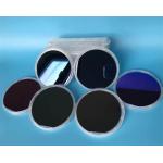
... growth 430um SSP DSP About synthetic sapphire crystal Due to the less mismatched lattice and stable chemical and physical properties, sapphire...
2025-07-30 00:08:00
|
|
...Sapphire Substrate wafers thickness 1.15mm C-a Sapphire application Application Sapphire wafer and substrate applications include: Microelectronic ...
2025-05-06 20:40:27
|
|
2-4inch Gallium antimonide GaSb Substrate Single Crystal Monocrystal for Semiconductor InAsSb/In-AsPSb, InNAsSb and other heterojunction materials can ...
2025-05-06 20:44:36
|