
261 - 270 of 315
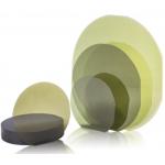
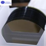
dsp sapphire substrate wafer
Selling leads
|
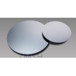
...wafer 1mm thickness for ingot growth Customzied size/2inch/3inch/4inch/6inch 6H-N/4H-SEMI/ 4H-N SIC ingots/High purity 4H-N 4inch 6inch dia 150mm ...
2025-05-06 20:40:54
|

|
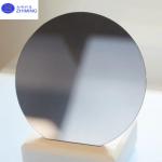
SapphiLarge Thickness Thermal Oxide (SiO2) On Silicon Wafers For Optical Communication System Generally, the oxide layer thickness of silicon wafers ...
2025-07-31 00:12:25
|
|
Electronic-Grade Silicon Wafers Ultra-High Purity Optoelectronic-Grade Abstract The high-purity silicon wafer we offer undergoes precision machining ...
2025-05-06 20:45:04
|
|
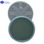
SOI wafers 4 Inches, 6 Inches, 8 Inches, Compatible with CMOS three-layer structure Product Description: The SOI (Silicon on Insulator) wafer stands ...
2025-05-06 20:45:07
|
|
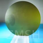
Epi ready 4inch InP wafers N-type p-type EPF<1000cm^2 with the thickness of 325um±50um Product abstract Our product, the "High-Purity Indium Phosphide ...
2025-05-06 20:45:10
|
|
SiC Substrate 4inch P-type 4H/6H-P N-type 3C-N Zero Grade Production Grade Dummy Grade P-type SiC Substrate's abstract P-type Silicon Carbide (SiC) ...
2025-05-06 20:41:40
|
|
...substrate 2 4 6 inch for 2.5~25G DFB laser diode InP DFB Epiwafer InP substrate's brief InP DFB Epiwafers designed for 1390nm wavelength applicatio...
2025-05-06 20:45:38
|
|
... optical applications, particularly for Gigabit Ethernet and digital data link communication. Built on a 6-inch wafer, it features a high ...
2025-05-06 20:45:39
|
|
The 6-inch Conductive Single-Crystal SiC on Polycrystalline SiC Composite Substrate Abstract of the 6-inch Conductive Single-Crystal SiC on Polycrysta...
2025-05-13 05:30:20
|
|
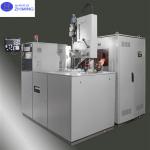
Sapphire Crystal Growth furnance KY Kyropoulos method 90-400kg for sapphire manufacture KY Sapphire Crystal Growth furnance's abstract This Sapphire ...
2025-05-06 20:43:46
|