
51 - 59 of 59
technical ceramic parts inp wafer
Selling leads
|
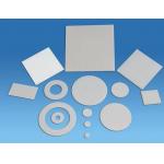
Substrates, Wafers From Technical Ceramics For The Electronics Industry Substrates based on Alumina (Al2O3), Aluminum nitride (AlN), Silicon nitride ...
2024-12-09 19:40:24
|

|
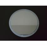
Thermal Oxide Wafer, higher uniformity, and higher dielectric strength , excellent dielectric layer as an insulator Thermal oxide or silicon dioxide ...
2024-12-09 13:28:02
|
|
GaAs Based Epi Wafer We provides MBE / MOCVD epitaxial growth of custom structure on GaAs substrate for microelectronics , optoelectronics and RF ...
2024-12-09 13:28:02
|
|
|
GaAs Based Epi Wafer We provides MBE / MOCVD epitaxial growth of custom structure on GaAs substrate for microelectronics , optoelectronics and RF ...
2024-12-09 19:40:24
|
|
|
Thermal Oxide Wafer, higher uniformity, and higher dielectric strength , excellent dielectric layer as an insulator Thermal oxide or silicon dioxide ...
2024-12-09 19:40:24
|
|
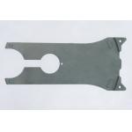
High precision silicon carbide components for semiconductor processes and optical machinery equipment Silicon carbide robotic arm is formed by ...
2024-12-09 13:24:42
|
|
|
High precision silicon carbide components for semiconductor processes and optical machinery equipment Silicon carbide robotic arm is formed by ...
2024-12-09 19:40:24
|
|
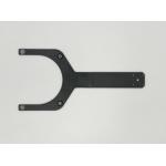
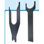
Resistance High Temperature SIC Fork Resistance High Temperature SIC Forks Core boost for semiconductor precision manufacturing. Materials: SiC finger ...
2025-05-13 07:41:06
|
|
High Corrosion Resistance SIC Finger SiC finger (fork) Application: SiC fingers are used in automation wafer transfer equipment which has been widely ...
2025-05-28 07:33:44
|