
Higher Uniformity Thermal Oxide Wafer Excellent Dielectric Layer As An Insulator
|
|
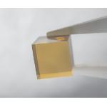
Thermal Oxide Wafer, higher uniformity, and higher dielectric strength , excellent dielectric layer as an insulator
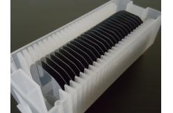
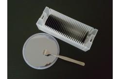
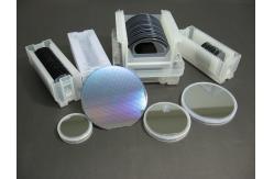
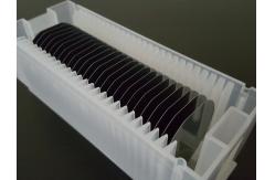
Thermal oxide or silicon dioxide layer is formed on bare silicon surface at elevated temperature in the presence of an oxidant , the process is called thermal oxidation. Thermal oxide is normally grown in a horizontal tube furnace , at temperature range from 900°C ~ 1200°C , using either a "Wet" or "Dry" growth method . Thermal oxide is a kind of "grown" oxide layer , compared to CVD deposited oxide layer , it has a higher uniformity, and higher dielectric strength , it is an excellent dielectric layer as an insulator . In most silicon- based devices, thermal oxide layer play an important role to pacify the silicon surface to act as doping barriers and as surface dielectrics . we provides thermal oxide wafer in diameter from 2" to 12 " , we always choose prime grade and defect free silicon wafer as substrate for growing high uniformity thermal oxide layer to meet your specific requirements . Contact us for further information on price & delivery time .
Thermal Oxide Capability Typically after thermal oxidation process , both front side and
back side of silicon wafer have oxide layer . In case only one side
oxide layer is required , we can remove back oxide and offer one
side thermal oxide wafer for you .
Thermal Oxide Wafer Application
Product Specification
|
||||||||||||||||||||||||||||||||||||||||||||||||||||||||||||||||||||
| Product Tags: Higher Uniformity Thermal Oxide Wafer Thermal Oxide Wafer as Insulator 2" thermal oxide silicon wafer |
|
High Concentration Quantum Grade Diamond Customized Size |
|
Single Crystal Diamond Cutting Tools Good Wear Resistance |
|
Indusatial Ceramics Parts Cultured Diamonds Pink Blue Yellow |
|
Diamond Heat Dissipation Material Thermal Management For Electronic Packaging Heat Dissipation |
|
Corseed Electrically Conductive Ceramics Handling Arm |
|
High Performance Nozzle Or Injector Technical Ceramic Parts |