
301 - 310 of 362
industrial ceramic sputtering target
Selling leads
|
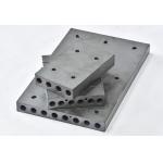
Silicon carbide heating plate Silicon carbide heating plate is formed by isostatic pressing and sintering at high temperature. According to the ...
2024-12-09 13:24:42
|
|
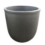
Silicon Carbide Graphite Crucible Silicon carbide crucible matching furnace type: it can be used for gas producer, gas furnace, coke oven, oil furnace...
2024-12-09 13:24:42
|
|
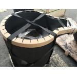
Silicon Carbide Graphite Spouted Crucible Silicon carbide crucible matching furnace type: it can be used for gas producer, gas furnace, coke oven, oil ...
2024-12-09 13:24:42
|
|
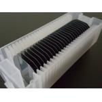
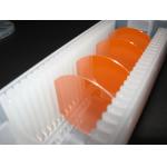
Single crystal and polycrystalline GaAs wafer ( Gallium Arsenide ) for making LD , LED , microwave circuit, solar cell We provides both single crystal ...
2024-12-09 13:28:02
|
|
Single Crystal GaP Wafer ( Gallium Phosphide ),widely used as red , yellow , and green LED ( light-emitting diodes ) We provides high quality single ...
2024-12-09 13:28:02
|
|
InAs wafer ( Indium Arsenide ) We provides InAs wafer ( Indium Arsenide ) to optoelectronics industry in diameter up to 2 inch . InAs crystal is a ...
2024-12-09 13:28:02
|

|
Sapphire Wafer, making blue LED , high Tc superconductor and microwave IC Semiconductor Wafer Inc. provides single crystal sapphire wafer to ...
2024-12-09 13:28:02
|
|
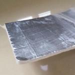
Aerogel Blanket Z200 Suitable for Low temperature freezing pipelines, equipment, vessels, storage tanks Description of Z200 Z200 series aerogel ...
2024-12-09 13:32:02
|
|
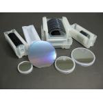
CE: luage, Scintillation crystal CE: luage: luag is an excellent scintillator with fast attenuation (80ns), high light yield and 510nm emission peak, ...
2024-12-09 13:42:48
|
|
LaAlO3 single crystal LaAlO3 single crystal is the most important industrial and large-scale high temperature superconducting thin film substrate ...
2024-12-09 13:42:48
|