
581 - 590 of 643
high performance ceramic resistors
Selling leads
|
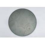
SiC PVD Tray Silicon carbide PVD tray is formed by isostatic pressing process and sintering at high temperature. The outer diameter, thickness, number ...
2024-12-09 13:24:42
|
|
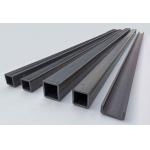
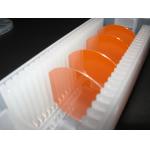
Silicon carbide square beams and semi-open square beams Silicon Carbide Square Beams are formed by high temperature sintering using an extrusion ...
2024-12-09 13:24:42
|
|
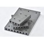
Silicon carbide heating plate Silicon carbide heating plate is formed by isostatic pressing and sintering at high temperature. According to the ...
2024-12-09 13:24:42
|

|
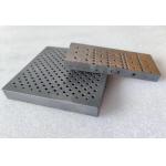
SiC Micro-Reaction Plate SiC micro-reaction plates are formed by isostatic pressing and sintering at high temperature.According to the special needs ...
2024-12-09 13:24:42
|
|
SiC Micro-reaction module SiC micro-reaction module is a multi-layer structure (usually 2 to 5 layers), which is composed of a reaction plate, a heat ...
2024-12-09 13:24:42
|
|
Single Crystal GaP Wafer ( Gallium Phosphide ),widely used as red , yellow , and green LED ( light-emitting diodes ) We provides high quality single ...
2024-12-09 13:28:02
|
|
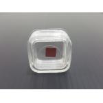
InAs wafer ( Indium Arsenide ) We provides InAs wafer ( Indium Arsenide ) to optoelectronics industry in diameter up to 2 inch . InAs crystal is a ...
2024-12-09 13:28:02
|
|
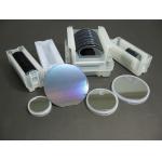
ZnO Wafer, CdS wafer, CdSe wafer, CdTe wafer, ZnS wafer, ZnSe wafer and ZnTe wafer We provides high purity single crystal ZnO wafer and ZnO bulk for ...
2024-12-09 13:28:02
|
|
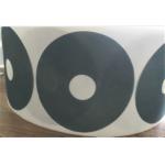
Microfinishing PSA Film Disc Roll, produce a fast cut-rate and uniform finish on wood, solid surface composites Microfinishing PSA Film Disc Roll ...
2024-12-09 13:28:37
|

|
Zirconia stirrers and tappets for glass production Zirconia is used to manufacture the components for glass production. Stirrers are used for ...
2024-12-09 13:37:42
|