
350um ZnO Wafer CdS CdSe CdTe ZnS ZnSe Wafer And ZnTe Wafer
|
|
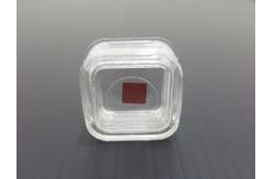
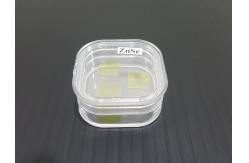
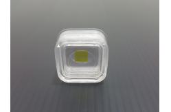
ZnO Wafer, CdS wafer, CdSe wafer, CdTe wafer, ZnS wafer, ZnSe wafer and ZnTe wafer
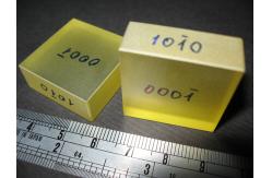
We provides high purity single crystal ZnO wafer and ZnO bulk for power device , LED , sensor and detector applications . With an ideal crystal structure , ZnO wafer ( Zinc oxide ) has a 2% lattice mismatch to GaN , that is much less than the lattice mismatch of sapphire wafer and SiC wafer . ZnO wafer is one of the most suitable substrate for using as GaN epitaxial growth and wide band gap semiconductor application . ZnO wafer are supplied in square shape , undoped , size 10 x 10 x 0.5 mm , double sides polished surface finish and oriented , our high quality ZnO wafer have been widely used for the growth of nitride base devices . Please contact us for more product information .
ZnO Wafer Application
ZnO Wafer Properties
Product Specification
|
||||||||||||||||||||||||||||||||||||
| Product Tags: 350um ZnO Wafer CdS CdSe ZnO Wafer 350um ZnTe Wafer |
|
Aluminum Nitride Structural Ceramic Parts High Strength |
|
Aluminum Nitride Ceramic Substrate High Thermal Conductivity |
|
High Pressure Pump Valve Assembly for Hydraulic Systems |
|
Ceramic Cylinder Liner Piston for Mud Pumps |

|
Trenchless Mudpump Ceramic Cylinder Liner |

|
Precision Ceramic Parts for Semiconductor Equipment |