
6-layer Hybrid PCB on RO3003 Substrate and 370HR Immersion Gold Circuits Board
|


|
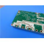
This custom six-layer hybrid PCB uses a mixed material of 5mil RO3003 high-frequency substrate and 5mil 370HR FR4. The finished board measures 0.82mm thick, with 1oz copper on outer layers and 0.5oz copper for inner layers. It uses blue solder mask printed with white silkscreen and immersion gold surface finish. The board size is 83mm × 42mm (1 piece). Key design features include 1-2 blind vias and 0.15mm through holes filled with copper paste.
PCB Specification The table below summarises all core manufacturing parameters for this hybrid PCB.
PCB Stack-up
Design Rationality of This 6-Layer Hybrid Dielectric Stack-up
1. Performance Advantages of 5mil RO3003 High-Frequency Laminate Combined with 370HR FR4 Hybrid Stack-up
The 5mil RO3003 substrate delivers low dielectric constant and low dissipation factor, keeping insertion loss minimal as microwave and RF signals travel across the circuit. For RF designs, signal loss directly degrades system sensitivity and operating range, so maintaining consistent low-loss behaviour is critical. The 5mil thin dielectric construction gives designers much finer control over impedance values for both single-ended and differential routing, which is essential when working with tightly defined RF circuit requirements.
Using 370HR high-Tg prepreg alongside RO3003 addresses the practical limitations that come with boards made entirely from ceramic-filled PTFE materials. 370HR’s robust thermal structure stands up to repeated SMT reflow cycles, resisting interlayer delamination even when assemblies go through multiple thermal runs. Building a full PTFE ceramic board for the whole stackup would push material costs far higher, while those pure high-frequency laminates also tend to struggle with thermal stability during assembly. By mixing RO3003 for RF signal layers with 370HR FR4 for the rest of the stack, the design preserves the electrical performance required for RF operation without overspending on raw materials. This balanced approach has made the RO3003 + 370HR hybrid stack a popular choice for many small and medium RF modules where both performance and commercial viability matter.
2. Process Control Points for 0.82mm Standard-Thickness 6-Layer Hybrid PCB Lamination The stack configuration using 5mil RO3003 paired with 5mil 370HR prepreg is carefully calculated to reach the target finished board thickness of 0.82 mm, with tight limits placed on thickness variation. Every starting material’s thickness and resin content must be verified before lamination, because inconsistent prepreg resin flow will shift the final board thickness outside acceptable tolerance.
RO3003 and 370HR FR4 have different thermal expansion behaviour, which creates the main manufacturing challenge for this hybrid build. RO3003 is ceramic-filled PTFE while 370HR is epoxy-based FR4; their expansion rates diverge when heated up and cooled down during pressing. To counter this mismatch, fabricators must adopt segmented heating lamination profiles. Slow ramp-up rates and controlled cooling phases help ease thermal stress between dissimilar materials, paired with specialised anti-delamination processes to prevent separation at the material interface.
This 6-layer PCB is only 0.82mm thick, so layer shift and board warpage are two of the most common production defects. Layer shift usually arises from uneven pressure distribution during lamination and inconsistent resin flow across the panel. Warpage happens when uneven thermal stress accumulates across dissimilar dielectric layers after cooling. To mitigate these issues, manufacturers use careful panel layout, balanced copper distribution, controlled pressure cycles and post-lamination stress relief steps. These targeted measures reduce reject rates and ensure the finished thin six-layer hybrid PCB meets dimensional and reliability requirements.
|
||||||||||||||||||
| Product Tags: Polyimide FR4 PCB 3-layer FPC PCB Immersion Gold PCB |

|
6-layer Hybrid PCB on RO3003 Substrate and 370HR Immersion Gold Circuits Board |

|
Hybrid PCB 4-layer RO4003C and FR4 Material 0.5oz/1oz Copper Green Solder Mask |
|
Hybrid PCB RO4350B and TU768 Substrate 10-layer Immersion Gold RF Circuit Board |

|
RO3003 + Tg170 FR-4 Hybrid 4-Layer PCB Ceramic-Filled PTFE High Frequency Circuit Board |

|
6-Layer RO4350B & IT180A Hybrid PCB 1.6mm Thick Blind Via & Edge Plating High Frequency Board |

|
4-Layer Rogers RT/duroid 6202 Hybrid PCB 1.014mm Gold Plated Circuit Board |