
21 - 30 of 224
ce direct imaging pcb
Selling leads

|
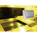
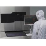
... direct imaging ( LDI ) exposes the traces directly with a highly focused laser beam that in NC controlled, instead of flooded light passing ...
2025-05-27 18:50:02
|
|
...direct imaging (LDI) system solutions PCB Solder Mask Difference between LDI and traditional exposure 1. Traditional exposure is to transfer the ...
2025-08-01 00:12:46
|
|
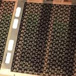
... PCB production efficiency and lower yields. Nowadays, an average PCB trace width reaches 0.075mm (3mil) in complex multilayer PCBs. While ...
2025-05-27 18:50:02
|
|
... direct imaging ( LDI ) exposes the traces directly with a highly focused laser beam that in NC controlled, instead of flooded light passing ...
2025-05-27 18:50:02
|
|
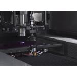
...direct imaging (LDI) system solutions PCB Solder Mask When fabricating a circuit board, the circuit traces are defined by what is the imaging ...
2025-05-27 18:50:02
|
|
... to the copper circuit pattern. It has been proved that LDI systems, which work in UV spectrum are most suitable for obtaining fine lines and ...
2025-05-27 18:50:02
|
|
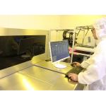
...consistently than traditional photo ways. The laser direct image process typically goes as follows: 1. Coat resist on the copper laminate; 2. ...
2025-05-27 18:50:02
|

|
...required to be replaced with a more sensitive dry film to achieve faster imaging speed, or the dry film is replaced with a different wavelength ...
2025-05-27 18:50:02
|
|
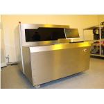
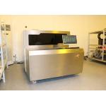
... Mixing Wave Laser Direct Imaging Circuit Board PAD Alignment 0.5~3.0mm Diameter Solder Mask Ink 30s@600x500mm Product Description: Laser Direct ...
2025-05-27 18:50:02
|
|
...direct imaging (LDI) system solutions PCB Solder Mask Advantages of LDI over photo processing When creating the photo tool for generating the image ...
2025-05-27 18:50:02
|