
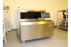
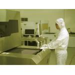
PCB Laser Direct Image HDI FPC 610mmx710mm ISO 9001
|
|
laser direct imaging (LDI) system solutions PCB Solder Mask
Now it will be a matter of updating the design file as changing to the necessary image, which can be done more cost-effectively and consistently than traditional photo ways. The laser direct image process typically goes as follows: 1. Coat resist on the copper laminate; 2. Exposing the photo of the PCB pattern on the resist; 3. Develop the unexposed resist; 4. Etch the exposed copper.
|
||||||||||||||||||||||||||||
| Product Tags: PCB laser direct image FPC laser direct image HDI ldi equipment |
|
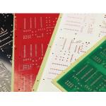
Laser Direct Imaging PCB With Scale Mode File Format For Application Of PCB HDI FPC |
|
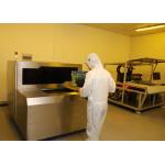
380V Three Phase Laser Direct Imaging PCB HDI FPC |
|
FPC HDI 50um Laser Direct Imaging Equipment 610x710mm |
|
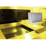
Laser Direct Imaging Printed Circuit Board With 30s@600x500mm Solder Mask Ink |
|
Laser Direct Imaging PCB Solder Mask For PCB、HDI、FPC With File Format |
|
File Format Laser Direct Imaging PCB With PAD Alignment Method 0.5~3.0mm Diameter |