
CE 610mmx710mm LDI Laser Direct Imaging Machine PCB
|

|
laser direct imaging (LDI) system solutions for various PCB Multilayer
When Opt to LDI Technology?
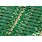
Existing technologies are unable to offer acceptable solution and the inevitable results is reduced PCB production efficiency and lower yields. Nowadays, an average PCB trace width reaches 0.075mm (3mil) in complex multilayer PCBs. While photolithography imaging process unfortunately reached its limits due to creating high density interconnects on PCB. It is unable to creating PCB below 0.127/0.127mm (5/5mil) of trace widths and spaces. So, when most of the trace widths and spaces on a circuit board are smaller than 0.127/0.127mm (5/5mil), LDI is the best imaging option.
LDI technology is mainly used in HDI board manufacturing before. But now PCB manufacturers have to manufacture fine-line and ultra-fine-line conventional rigid, flex and rigid-flex PCBs with LDI technology where the trace widths and spaces of the conductive circuits are 0.075/0.075mm (3/3mil) or even 0.05/0.05mm (2/2mil). That’s because Laser Direct Imaging (LDI) has proved itself as the best and most comprehensive imaging solution for fine trace widths and spaces.
How does laser direct imaging ( LDI ) work?
|
||||||||||||||||||||||||||||
| Product Tags: 610mm laser direct imaging machine CE PCB laser direct imaging machine CE direct imaging pcb |
|
HDI FPC LDI Laser Direct Imaging 610mmx710mm For Various PCB Multilayer |
|
380V Three Phase LDI Laser Direct Imaging Equipment 30um |
|
ISO 9001 CE LDI Laser Direct Imaging PCB 0.05mm-3.5mm |

|
610mmx710mm LDI Laser Direct Imaging PCB HDI FPC 380V Three Phase |
|
24um 380V Three Phase PCB LDI Laser Direct Imaging ISO 9001 CE LD Laser |

|
PCB HDI FPC LDI Laser Direct Imaging 610mmx710mm |