
121 - 130 of 179
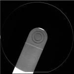
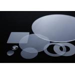
polished lithium niobate wafer
Selling leads
|
... stress, an electric field or charge proportional to the stress will be generated. This phenomenon is called the positive piezoelectric effect. ...
2024-12-09 20:57:43
|
|
.... It has an orientation of ±0.5°, a wafer shape, a clear aperture of greater than 90%, and TTV of ≤3μm. It is also customizable in size to meet the ...
2024-12-09 23:10:26
|

|
Diameter 6inch Sapphire Wafer LED Grade Polished Transparent Product Description: Sapphire Wafer is a high-precision sapphire substrate with superior ...
2024-12-09 23:10:26
|
|
Diameter 4inch Sapphire Wafer grade with Single Side Polished Surface Quality Product Description: Sapphire Wafer – The Ultimate Sapphire Plate ...
2024-12-09 23:10:26
|
|
...Wafer and BF33 C7980 BK7 H-K9L Glass Wafers The glass wafers are widely used as bonding material with silicon wafers in semiconductor industry. ...
2024-12-09 20:34:25
|
|
..., chemically etched or polished. The cut angles mostly used are: family of AT-cuts, BT-cut, CT-cut, DT-cut, X-cut and Y-cut. They are used for ...
2025-08-03 00:13:22
|
|
...Polished Sapphire Wafers Sapphire Substrates Specification: Single crystal Al2O3 99.999% Orientation: R-axis 0.5° Diameter:50.8±0.1mm Thickness ...
2024-12-09 21:21:54
|
|
...Polished High-Performance Sapphire Al2O3 Crystal Substrate Ultrathin 2" 3" 4" Sapphire wafers are the epitome of modern semiconductor technology, ...
2024-12-09 21:17:37
|
|
2 Inch C Plane 0001 430um Sapphire Single Crystal Wafers Polished Wafer Sapphire is a single crystal of alumina and is the second-hardest material in ...
2024-12-09 21:35:54
|
|
... unparalleled durability and exceptional optical properties. Ideal for a range of applications including optics, sensors, and high-end jewelry, ...
2024-12-09 23:27:58
|