
91 - 100 of 371
optoelectronic applications piezoelectric wafer
Selling leads
|
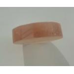
..., wear resistance, corrosion resistance and high temperature and high pressure resistance, biocompatibility, is an ideal substrate material for the ...
2024-12-09 21:35:54
|
|
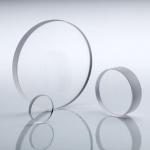
... applications. Our standard wafer diameters range from 25.4 mm (1 inch) to 150 mm (6 inches) in size. Lithium Tantalate (LiTaO3), also known as LN ...
2025-07-23 00:16:00
|
|
.... Such wafers are most commonly specified as 3" diameter with a reference flat. Wafer orientation is customer specified based on desired component ...
2025-07-23 00:16:00
|
|
Unleash the Full Potential of Your Optoelectronic Devices with Our High Thermal Conductivity MgO Single Crystal Substrate Introducing our premium MgO ...
2025-06-28 00:24:28
|
|
... requiring exceptional piezoelectric, ferroelectric, and optical properties. These wafers, crafted from the highest purity stoichiometric lithium ...
2025-03-06 16:31:02
|
|
...Piezoelectric Wafers with Differnent Cut Angles and Propagation Directions The word piezoelectric originates from the Greek word piezein, which ...
2024-12-09 20:34:25
|
|
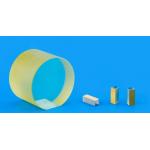
Customized 6 Inch 8 Inch Piezoelectric Wafer for Semiconductor POI and MEMS Positive piezoelectric effect (direct piezoelectric effect) : The ...
2024-12-09 20:34:25
|
|
... that have this property fall under the category "piezoelectric." Mechanical or electrical energy can be applied to the same piezoelectedrical ...
2024-12-09 20:34:25
|
|
...Piezoelectric LiNbO3 LiT Wafers widely used in Telecommunications Lithium Tantalate (LT, LiTaO3) has unique properties, which as a material finds ...
2025-07-23 00:16:00
|
|
...Wafers The Ultimate Solution for High-Speed Data Transmission Optical Signal Processing The power of our premium LiNbO3 Wafers, the cornerstone for ...
2025-03-06 16:30:59
|