
101 - 110 of 371
optoelectronic applications piezoelectric wafer
Selling leads

|
...Wafer for Superior SAW Device Performance Lithium niobate wafers are revolutionizing the optical technology industry with their unique combination ...
2024-12-09 20:34:25
|

|
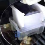
Customizable doping percent LiNbO3 Wafer MgO Er Fe doped Optical grade or SAW grade Lithium Niobate (LiNbO3) is a useful optoelectronic material. The ...
2025-07-23 00:16:00
|
|
Customized doping percent LiNbO3 Wafer MgO Er Fe doped Optical grade or SAW grade Lithium Niobate (LiNbO3) is a useful optoelectronic material. The ...
2024-12-09 20:34:25
|
|
Fe doped Lithium Niobate Wafer Optical Grade and SAW Grade Lithium Niobate (LiNbO3) is a useful optoelectronic material. The material not only has ...
2025-07-23 00:16:00
|
|
...TTV of ≤3μm, thickness of 0.5mm-3mm and roundness of edge grinding. With its high-end material and strict quality control, Sapphire Wafer provides ...
2024-12-09 23:10:26
|
|
...Wafer with A-plane 11-20 Primary Flat Our sapphire wafers are precision-crafted using the finest materials and cutting-edge technology. Sapphire, a ...
2024-12-09 20:34:25
|
|
...Wafer with Superior Thermal and Optical Properties semiconductor and optical industries. Crafted from the purest quartz minerals, our wafers boast ...
2025-07-23 00:16:00
|
|
...Wafer with High Refractive Index for SAW Sensor and Frequency Converter The Ultimate Material for Precision Applications LiTaO3, a revolutionary ...
2024-12-09 23:45:42
|
|
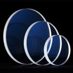
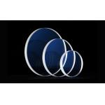
Piezoelectric Ring Lithium Niobate Wafer Orientation 36Y-Cut Customization Lithium Niobate (LN) is a ferroelectric material with excellent electro...
2025-07-23 00:16:00
|
|
... is subjected to mechanical stress, an electric field or charge proportional to the stress will be generated. This phenomenon is called the ...
2024-12-09 20:57:43
|