
101 - 110 of 161
high temperature use langasite wafers
Selling leads
|
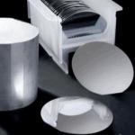
...r specific requirements are met by choosing prime grade and defecting free silicon wafer as a substrate so that a high uniform layer of thermal ...
2025-07-26 00:13:55
|
|
... even if the electric potential occurs instantaneously. The pyroelectric effect of LN wafer is almost eliminated and the transmittance is ...
2025-07-26 00:13:55
|
|
... are made from high-purity lithium niobate crystals and offer several advantages due to their larger size. Here is a description of 8-inch LiNbO3 ...
2024-12-09 22:36:19
|
|
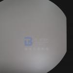
...TTV of ≤3μm, thickness of 0.5mm-3mm and roundness of edge grinding. With its high-end material and strict quality control, Sapphire Wafer provides ...
2024-12-09 23:10:26
|
|
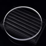
Semiconductor use Fused Silica Wafer with Low CTE for UV Lithography Wafers from semiconductor grade quartz (amorphous) are used in semiconductor ...
2024-12-09 20:34:25
|
|
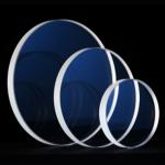
...Wafer for High Frequency Broadband Filter and Piezoelectric Transducer The electromechanical coupling coefficient of LiTaO3 crystals is large, and ...
2024-12-09 21:17:37
|
|
...Description: Fused Silica Wafer is a high-performance, cost-effective IC Silicon Wafer product that is widely used in the semiconductor, MEMS and ...
2024-12-09 22:58:07
|
|
...Wafer Used As Infrared Windows Night Infrared Scope Night Vision Camera Sapphire wafers are the epitome of modern semiconductor technology, ...
2024-12-09 20:34:25
|
|
... that non-doped lithium niobate exhibits high photorefraction. Therefore in high-power laser applications, magnesium oxide-doped crystals (MgO...
2025-07-26 00:13:55
|
|
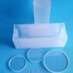
...an ideal material for Anodic bonding. BonTek provides borosilicate wafers from 2 to 14 inches diameter, the thickness is 100um up with low ...
2024-12-09 20:34:25
|