
171 - 180 of 217
electrical optical timing piezoelectric wafer
Selling leads
|
...Wafer SAW Application IDT use Ra Roughness 1nm The reduction technology is used to produce Black Lithium Niobate (LiNbO3) which has high ability to ...
2024-12-09 20:34:25
|
|
...Wafer used in Visible, Near-Infrared and Mid-Infrared Regions Lithium niobate is transparent between 0.25 and 5.3 μm. It can be used in visible, ...
2025-08-01 00:14:26
|
|
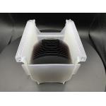
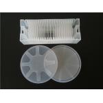
...Wafer 64Y 128Y Single Side Polished For SAW Lithium niobate has good nonlinear optical properties, so it can be used as optical waveguide material, ...
2025-08-01 00:14:26
|
|
...Wafer used in Visible, Near-Infrared and Mid-Infrared Regions Lithium niobate is transparent between 0.25 and 5.3 μm. It can be used in visible, ...
2024-12-09 20:34:25
|
|
..., electronics, and beyond. This unique crystalline compound boasts an exceptional combination of properties, making it a cornerstone in modern ...
2024-12-10 00:15:50
|
|
...optoelectronic applications. Stoichiometric LiTaO3, renowned for its exceptional ferroelectric, piezoelectric, and electro-optic properties, is the ...
2024-12-10 00:31:18
|
|
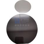
3 Inch Dia 76.2mm Sapphire Substrate Optical Crystal Windows Single crystal sapphire Al2O3 possesses a unique combination of excellent optical, ...
2024-12-09 21:35:54
|
|
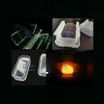
... even if the electric potential occurs instantaneously. The pyroelectric effect of LN wafer is almost eliminated and the transmittance is ...
2025-08-01 00:14:26
|
|
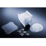
...precision and durability, our single-crystal quartz wafers are the ideal solution. These wafers, crafted from pure quartz, exhibit exceptional ...
2025-08-01 00:14:26
|
|
... feature is that its atoms or molecules are arranged regularly, which reflects the symmetry of the shape on a macroscopic scale. Under the action ...
2025-08-01 00:14:26
|