
11 - 20 of 88
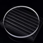
custom silica wafer
Selling leads
|
...Fused Silica Wafer 3'' 4'' 6'' JGS1 JGS2 JGS3 for Glass and Quartz Materials The Epitome of Optical Clarity and Precision Elevate your optical ...
2025-07-23 00:16:00
|
|
... in the VIS and UV is approx. The transmission range of significantly cheaper JGS2 wafers is shifted towards longer wavelengths when compared with ...
2024-12-09 20:34:25
|
|
UV grade Fused Silica Wafer customized Diameter Thickness JGS1 JGS2 JGS3 BonTek works on a variety of glass and quartz materials depending on the ...
2025-07-23 00:16:00
|

|
... Silica Wafer in Infrared and Ultraviolet Spectrum Fused Silica or Fused Quartz which is the amorphous phase of quartz (SiO2). When contrasted to ...
2025-07-23 00:16:00
|
|
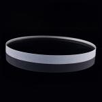
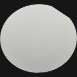
Product Description: Fused Silica Wafer is an optical-grade monocrystalline wafer made of quartz material, also known as fused quartz or fused silica. ...
2024-12-09 22:58:07
|
|
... applications. Crafted from the purest fused silica, our wafers offer unparalleled optical clarity, thermal stability, and chemical resistance. ...
2024-12-10 00:15:50
|
|
Semiconductor use Fused Silica Wafer with Low CTE for UV Lithography Wafers from semiconductor grade quartz (amorphous) are used in semiconductor ...
2024-12-09 20:34:25
|
|
Product Description: Fused Silica Wafer is a high-performance, cost-effective IC Silicon Wafer product that is widely used in the semiconductor, MEMS ...
2024-12-09 22:58:07
|
|
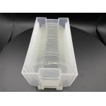
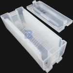
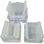
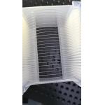
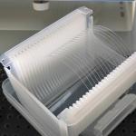
...Silica Quartz Borosilicate Glass Wafer As Carrier Wafers Due to their low thickness, thin wafers are vulnerable to stress and breakage. Warping of ...
2025-07-23 00:16:00
|
|
... component must meet the strictest standards. That's where our Fused Silica Wafers shine, offering a level of quality and performance that sets ...
2025-06-28 00:24:28
|