
IC Substrate Multilayer Rigid PCB for Mobile Phone EMMC Package Substrate
|
|
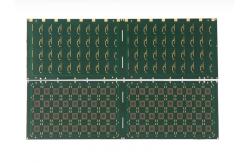
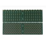
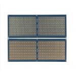
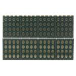
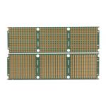
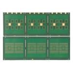
Product Images
About TECircuit
Found: TECircuit has been operating since 2004.
Product Applications
Product Features
FAQ Question 1: What is needed for a quotation? Product Description
|
||||||||||||||||||||||||||||||||||||||||||||||||||||||||||||||||||||||||||||||||||||||||||||||||||||||||||||||||||||||||||||||||||||||||||||||||||||||||||||
| Product Tags: Mobile Phone Multilayer Rigid PCB IC Substrate Mobile Phone PCB | ||||||||||||||||||||||||||||||||||||||||||||||||||||||||||||||||||||||||||||||||||||||||||||||||||||||||||||||||||||||||||||||||||||||||||||||||||||||||||||
|
IC Substrate Multilayer Rigid PCB for Mobile Phone EMMC Package Substrate |
|
IC Substrate PCB Multilayer Rigid Printed Circuit Board LGA Package ENIG Finish |
|
Multilayer Rigid IC Substrate PCB Board Fingerprint Card Soft Gold Hard Gold |
|
IC Substrate Multilayer Rigid PCB MEMS Sensor Micro Electromechanical System |

|
IC Substrate Multilayer PCB , HDI Rigid PCB ENIG Surface for RF Module |
|
Multilayer IC Substrate PCB Board PCB Rigid Blind Vias Soft Gold |