
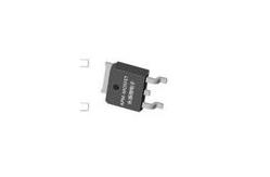
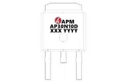
AP30N10D High Current Transistor , 30A 100V TO-252 Field Effect Transistor
|
|
AP30N10D High Current Transistor , 30A 100V TO-252 Field Effect Transistor
High Current Transistor types
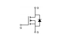
MOSFETs can be of different types, including:
Depletion Mode: Normally ON. Applying the VGS would turn it OFF. Enhancement Mode: Normally OFF. Applying the VGS would turn it ON. N-channel MOSFETs: positive voltages and currents. P-channel MOSFETs: negative voltages and currents. Low voltage MOSFETs: BVDSS from 0 V to 200 V. High voltage MOSFETs: BVDSS greather than 200 V.
High Current Transistor Features
VDS = 100V ID = 30A
High Current Transistor usage
Battery protection
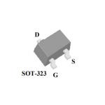
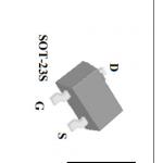
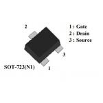
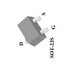
Package Marking and Ordering Information
Absolute Maximum Ratings Tc=25℃ unless otherwise noted
Note : 1.The data tested by surface mounted on a 1 inch FR-4 board with 2OZ copper. 2.The data tested by pulsed , pulse width ≦ 300us , duty cycle ≦ 2% 3.The EAS data shows Max. rating . The test condition is VDD=25V,VGS=10V,L=0.1mH,IAS =27A 4.The power dissipation is limited by 150℃ junction temperature 5.The data is theoretically the same as IDand IDM, in real applications , should be limited by total power dissipation.
Attention
1, Any and all APM Microelectronics products described or contained herein do not have specifications that can handle applications that require extremely high levels of reliability, such as life support systems, aircraft's control systems, or other applications whose failure can be reasonably expected to result in serious physical and/or material damage. Consult with your APM Microelectronics representative nearest you before using any APM Microelectronics products described or contained herein in such applications. 2, APM Microelectronics assumes no responsibility for equipment failures that result from using products at values that exceed, even momentarily, rated values (such as maximum ratings, operating condition ranges, or other parameters) listed in products specifications of any and all APM Microelectronics products described or contained herein. 3, Specifications of any and all APM Microelectronics products described or contained here instipulate the performance, characteristics, and functions of the described products in the independent state, and are not guarantees of the performance, characteristics, and functions of the described products as mounted in the customer’s products or equipment. To verify symptoms and states that cannot be evaluated in an independent device, the customer should always evaluate and test devices mounted in the customer’s products or equipment. 4, APM Microelectronics Semiconductor CO., LTD. strives to supply high quality high reliability products. However, any and all semiconductor products fail with some probability. It is possible that these probabilistic failures could give rise to accidents or events that could endanger human lives that could give rise to smoke or fire, or that could cause damage to other property. Whendesigning equipment, adopt safety measures so that these kinds of accidents or events cannot occur. Such measures include but are not limited to protective circuits and error prevention circuits for safe design, redundant design,and structural design. 5,In the event that any or all APM Microelectronics products(including technical data, services) described or contained herein are controlled under any of applicable local export control laws and regulations, such products must not be exported without obtaining the export license from the authorities concerned in accordance with the above law. 6, No part of this publication may be reproduced or transmitted in any form or by any means,electronic or mechanical, including photocopying and recording, or any information storage or retrieval system, or otherwise, without the prior written permission of APM Microelectronics Semiconductor CO., LTD. 7, Information (including circuit diagrams and circuit parameters) herein is for example only; it is not guaranteed for volume production. APM Microelectronics believes information herein is accurate and reliable, but no guarantees are made or implied regarding its use or any infringements of intellectual property rights or other rights of third parties. 8, Any and all information described or contained herein are subject to change without notice due to product/technology improvement,etc. When designing equipment, refer to the "Delivery Specification" for the APM Microelectronics product that you Intend to use.
|
||||||||||||||||||||||||||||||||||||||||||||||||||||||||||||||||||||||||||||||||||||||||||||||||||||||||||||||||||||||||||||||||||||||||||||||||||||||||||||||||||||||||||||||||||||||||||||||||||||||||||||||||||||||||||||||||||||||||||||||||||||||||||||||||||||||||||||||||||||||||||||||||||||||||||||||||||||||||||||||||||||||||||||||||||||||||||||||||||||||||||||||||||||||||||||||||||||||||||||||||||||
| Product Tags: n channel mosfet transistor high voltage transistor |
|
AP2602GY-HF FR4 board 2W 30A SOT-26 IC Voltage Regulator |
|
LED Inductor 0.35W 2.5A Mosfet Power Transistor AP1332GEU-HF |
|
Drive IC AP2308GEN SOT-23 0.69W 3.6A Mosfet Power Transistor |
|
AP2N1K2EN1 IC Chips SOT-723 0.15W 800mA MOSFET Transistor |
|
AP2322GN LOGIC ICS 0.833W 10A MOSFET Power Switch |
|
AP1334GEU-HF 0.35W 8A Mosfet Power Transistor New Condition |