China Mosfet Power Transistor manufacturer
Shenzhen Hua Xuan Yang Electronics Co.,Ltd
Shenzhen Hua Xuan Yang Electronics Co.,Ltd Our electronic components semiconductor is your most correct choice, because we are professional, honest, high quality, low price
7
Home > Products > Mosfet Power Transistor >

High Frequency Mosfet Power Transistor 12N10 N Channel Low Gate Charge

Browse Categories

Shenzhen Hua Xuan Yang Electronics Co.,Ltd

City: shenzhen

Province/State:guangdong

Country/Region:china

Tel:+86--13417075252

Contact Person:
Mr.David Lee
View Contact Details

High Frequency Mosfet Power Transistor 12N10 N Channel Low Gate Charge

Brand Name Hua Xuan Yang
Model Number 12N10
Certification RoHS、SGS
Place of Origin ShenZhen China
Minimum Order Quantity 1000-2000 PCS
Price Negotiated
Payment Terms L/C T/T Western Union
Supply Ability 18,000,000PCS / Per Day
Delivery Time 1 - 2 Weeks
Packaging Details Boxed
Product name Mosfet Power Transistor
APPLICATION Power Management
FEATURE Excellent RDS(on)
Power mosfet transistor Enhancement Mode Power MOSFET
Detailed Product Description

HXY12N10 N-Channel Enhancement Mode Power MOSFET


DESCRIPTION

The HXY12N10 uses advanced trench technology and design to provide excellent RDS(ON) with low gate charge. It can be used in a wide variety of applications.


FEATURES

● VDS =100V,ID =12A

RDS(ON) < 130mΩ @ VGS =10V


Application


● Power switching application

● Hard switched and high frequency circuits

● Uninterruptible power supply


ORDERING INFORMATION

ParameterSymbolLimitUnit
Drain-Source VoltageVDS100V
Gate-Source VoltageVGS±20V
Drain Current-ContinuousID12A
Drain Current-Continuous(TC=100℃)ID (100℃)6.5A
Pulsed Drain CurrentIDM38.4A
Maximum Power DissipationPD30W
Derating factor 0.2W/℃
Single pulse avalanche energy (Note 5)EAS20mJ
Operating Junction and Storage Temperature RangeTJ,TSTG-55 To 175


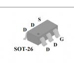
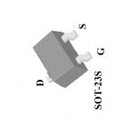
Note: Pin Assignment: G: Gate D: Drain S: Source


ABSOLUTE MAXIMUM RATINGS (TC = 25°С, unless otherwise specified)

PARAMETERSYMBOLRATINGSUNIT
Drain-Source VoltageVDSS600V
Gate-Source VoltageVGSS±30V
Continuous Drain CurrentID10A
Pulsed Drain Current (Note 2)IDM40A
Avalanche Current (Note 2)IAR8.0A
Avalanche EnergySingle Pulsed (Note 3)EAS365mJ
Peak Diode Recovery dv/dt (Note 4)dv/dt4.5ns


Power Dissipation

TO-220


PD

156W
 TO-220F1 50W
 TO-220F2 52W
Junction TemperatureTJ+150°C
Storage TemperatureTSTG-55 ~ +150°C

Notes: 1. Absolute maximum ratings are those values beyond which the device could be permanently damaged.

Absolute maximum ratings are stress ratings only and functional device operation is not implied.

4. Repetitive Rating: Pulse width limited by maximum junction temperature.

5. L = 84mH, IAS =1.4A, VDD = 50V, RG = 25 Ω Starting TJ = 25°C

6. ISD ≤ 2.0A, di/dt ≤200A/μs, VDD ≤BVDSS, Starting TJ = 25°C


ELECTRICAL CHARACTERISTICS (TJ = 25°С, unless otherwise specified)


ParameterSymbolConditionMinTypMaxUnit
Off Characteristics
Drain-Source Breakdown VoltageBVDSSVGS=0V ID=250μA100110-V
Zero Gate Voltage Drain CurrentIDSSVDS=100V,VGS=0V--1μA
Gate-Body Leakage CurrentIGSSVGS=±20V,VDS=0V--±100nA
On Characteristics (Note 3)
Gate Threshold VoltageVGS(th)VDS=VGS,ID=250μA1.21.82.5V
Drain-Source On-State ResistanceRDS(ON)VGS=10V, ID =8A98 130m Ω
Forward TransconductancegFSVDS=25V,ID=6A3.5--S
Dynamic Characteristics (Note4)
Input CapacitanceClss


VDS=25V,VGS=0V, F=1.0MHz

-690-PF
Output CapacitanceCoss -120-PF
Reverse Transfer CapacitanceCrss -90-PF
Switching Characteristics (Note 4)
Turn-on Delay Timetd(on)


VDD=30V,ID=2A,RL=15Ω VGS=10V,RG=2.5Ω

-11-nS
Turn-on Rise Timetr -7.4-nS
Turn-Off Delay Timetd(off) -35-nS
Turn-Off Fall Timetf -9.1-nS
Total Gate ChargeQg


VDS=30V,ID=3A, VGS=10V

-15.5 nC
Gate-Source ChargeQgs -3.2-nC
Gate-Drain ChargeQgd -4.7-nC
Drain-Source Diode Characteristics
Diode Forward Voltage (Note 3)VSDVGS=0V,IS=9.6A--1.2V
Diode Forward Current (Note 2)IS --9.6A
Reverse Recovery Timetrr

TJ = 25°C, IF =9.6A

di/dt = 100A/μs(Note3)

-21 nS
Reverse Recovery ChargeQrr -97 nC
Forward Turn-On TimetonIntrinsic turn-on time is negligible (turn-on is dominated by LS+LD)


Essentially independent of operating temperature.Notes: 1. Pulse Test : Pulse width ≤ 300µs, Duty cycle ≤ 2%.


Product Tags: n channel mosfet transistor   high voltage transistor  
Related Products
Email to this supplier
 
From:
Enter your Email please.
To: Shenzhen Hua Xuan Yang Electronics Co.,Ltd
Subject:
Message:
Characters Remaining: (80/3000)