China Mosfet Power Transistor manufacturer
Shenzhen Hua Xuan Yang Electronics Co.,Ltd
Shenzhen Hua Xuan Yang Electronics Co.,Ltd Our electronic components semiconductor is your most correct choice, because we are professional, honest, high quality, low price
7
Home > Products > Mosfet Power Transistor >

AP6H03S Mosfet Driver Using Transistor , Durable High Amp Transistor

Browse Categories

Shenzhen Hua Xuan Yang Electronics Co.,Ltd

City: shenzhen

Province/State:guangdong

Country/Region:china

Tel:+86--13417075252

Contact Person:
Mr.David Lee
View Contact Details

AP6H03S Mosfet Driver Using Transistor , Durable High Amp Transistor

Brand Name Hua Xuan Yang
Model Number AP6H03S
Certification RoHS、SGS
Place of Origin ShenZhen China
Minimum Order Quantity Negotiation
Price Negotiated
Payment Terms L/C T/T Western Union
Supply Ability 18,000,000PCS / Per Day
Delivery Time 1 - 2 Weeks
Packaging Details Boxed
Product name Mosfet Driver Using Transistor
Model AP6H03S
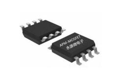
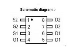
Pack SOP-8
Marking AP6H03S YYWWWW
VDSDrain-Source Voltage 30V
VGSGate-Sou rce Voltage ±20A
Detailed Product Description

AP6H03S Mosfet Driver Using Transistor , Durable High Amp Transistor


Mosfet Driver Using Transistor Description:


The AP6H03Suses advanced trench
technology to provide excellent RDS(ON) and low gate charge .
The complementary MOSFETs may be used to form a
level shifted high side switch, and for a host of other
applications


Mosfet Driver Using Transistor Features

N-Channel
VDS = 30V,ID =7.5A
RDS(ON) < 16mΩ@ VGS=10V
NChannel
VDS = 30V,ID =7.5A
RDS(ON) < 16mΩ@ VGS=10V
High power and current handing capability
Lead free product is acquired
Surface mount package


Mosfet Driver Using Transistor Application


● Hard Switched and High Frequency Circuits
● Uninterruptible Power Supply


Package Marking and Ordering Information


Product IDPackMarkingQty(PCS)
AP6H03SSOP-8AP6H03S YYWWWW3000


Absolute Maximum Ratings Tc=25℃ unless otherwise noted


SymbolParameterRatingUnits
VDSDrain-Source Voltage30V
VGSGate-Sou rce Voltage±20V


D

I

Drain Current – Continuous (TC=25℃)7.5A
Drain Current – Continuous (TC=100℃)4.8A
IDMDrain Current – Pulsed130A
EASSingle Pulse Avalanche Energy 214mJ
IASSingle Pulse Avalanched Current 217A


PD

Power Dissipation (TC=25℃)2.1W
Power Dissipation – Derate above 25℃0.017W/℃
TSTGStorage Temperature Range-55 to 150
TJOperating Junction Temperature Range-55 to 150


Thermal Characteristics


SymbolParameterTyp.Max.Unit
RθJAThermal Resistance Junction to ambient---60℃/W


Electrical Characteristics (TJ=25, unless otherwise noted) Off Characteristics


SymbolParameterConditionsMin.Typ.Max.Unit
BVDSSDrain-Source Breakdown VoltageVGS=0V , ID=250uA30------V
△ BVDSS/△ TJBVDSS Temperature CoefficientReference to 25℃•, ID=1mA---0.04---V/℃


IDSS


Drain-Source Leakage Current

VDS=30V , VGS=0V , TJ=25℃------1uA
VDS=24V , VGS=0V , TJ=125℃------10uA
IGSSGate-Source Leakage CurrentVGS=± 20V , VDS=0V------± 100nA


RDS(ON)Static Drain-Source On-ResistanceVGS=10V , ID=6A---1520
VGS=4.5V , ID=3A---2330
VGS(th)Gate Threshold VoltageVGS=VDS , I =250uA1.21.52.5V
△VGS(th)VGS(th) Temperature Coefficient----4---mV/℃
gfsForward TransconductanceVDS=10V , I D=6A---13---S


QgTotal Gate Charge3 , 4 ---4.18 
QgsGate-Source Charge 3 , 4---12
QgdGate-Drain Charge---2.14
Td(on)Turn-On Delay Time 3 , 4 ---2.65 
TrRise Time---7.214
Td(off)Turn-Off Delay Time 3 , 4---15.830
TfFall Time 3 , 4---4.69
CissInput Capacitance ---345500 
CossOutput Capacitance---5580
CrssReverse Transfer Capacitance---3255
RgGate resistanceVGS=0V, VDS=0V, f=1MHz---3.26.4Ω


ISContinuous Source Current


VG=VD=0V , Force Current

------7.5A
ISMPulsed Source Current------30A
VSDDiode Forward Voltage3VGS=0V , IS=1A , TJ=25℃------1V

rr

t

Reverse Recovery TimeVGS=0V,IS=1A , di/dt=100A/µs---------ns
QrrReverse Recovery Charge---------nC
ISContinuous Source Current


VG=VD=0V , Force Current

------7.5A
ISMPulsed Source Current------30A
VSDDiode Forward Voltage3VGS=0V , IS=1A , TJ=25℃------1V

rr

t

Reverse Recovery TimeVGS=0V,IS=1A , di/dt=100A/µs---------ns
QrrReverse Recovery Charge---------nC


Reflow Soldering

The choice of heating method may be influenced by plastic QFP package). If infrared or vapor phase heating is used and the package is not absolutely dry (less than 0.1% moisture content by weight), vaporization of the small amount of moisture in them can cause cracking of the plastic body. Preheating is necessary to dry the paste and evaporate the binding agent. Preheating duration: 45 minutes at 45 °C.


Reflow soldering requires solder paste (a suspension of fine solder particles, flux and binding agent) to be applied to the printed-circuit board by screen printing, stenciling or pressure-syringe dispensing before package placement. Several methods exist for reflowing; for example, convection or convection/infrared heating in a conveyor type oven. Throughput times (preheating, soldering and cooling) vary between 100 and 200 seconds depending on heating method.


Typical reflow peak temperatures range from 215 to 270 °C depending on solder paste material. The top-surface

temperature of the packages should preferable be kept below 245 °C for thick/large packages (packages with a thickness

2.5 mm or with a volume 350 mm so called thick/large packages). The top-surface temperature of the packages should preferable be kept below 260 °C for thin/small packages (packages with a thickness < 2.5 mm and a volume < 350 mm so called thin/small packages).


1’st Ram Up Ratemax3.0+/-2 /sec-
Preheat150 ~20060~180 sec
2’nd Ram Upmax3.0+/-2 /sec-
Solder Joint217 above60~150 sec
Peak Temp260 +0/-520~40 sec
Ram Down rate6 /sec max-

Wave Soldering:

Conventional single wave soldering is not recommended for surface mount devices (SMDs) or printed-circuit boards with a high component density, as solder bridging and non-wetting can present major problems.


Manual Soldering:

Fix the component by first soldering two diagonally-opposite end leads. Use a low voltage (24 V or less) soldering iron applied to the flat part of the lead. Contact time must be limited to 10 seconds at up to 300 °C. When using a dedicated tool, all other leads can be soldered in one operation within 2 to 5 seconds between 270 and 320 °C.


Product Tags: n channel mosfet transistor   high voltage transistor  
Related Products
Email to this supplier
 
From:
Enter your Email please.
To: Shenzhen Hua Xuan Yang Electronics Co.,Ltd
Subject:
Message:
Characters Remaining: (80/3000)