
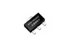
AP5N10SI N Channel Mosfet Power Transistor For Battery Powered System
|
|
AP5N10SI N Channel Mosfet Power Transistor For Battery Powered System
N Channel Mosfet Power Transistor Description:
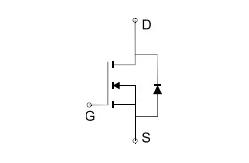
The AP5N10SI is the single N-Channel logic enhancement mode power field effect transistors to provide excellent R DS(on), low gate charge and low gate resistance. It ’s up to 30V operation voltage is well suited in switching mode power supply, SMPS, notebook computer power management and other battery powered circuits.
N Channel Mosfet Power Transistor Features:
RDS(ON)<125m Ω @VGS=10V (N-Ch) RDS(ON)<135mΩ @VGS =4.5V (N-Ch) Super high density cell design for extremely low RDS(ON) Exceptional on-resistance and maximum DC current
N Channel Mosfet Power Transistor Applications:
Switching power supply, SMPS Battery Powered System DC/DC Converter DC/AC Converter Load Switch
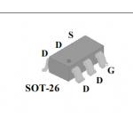
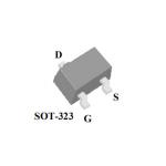
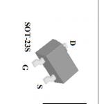
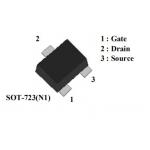
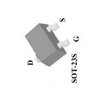
Package Marking and Ordering Information
Table 1.Absolute Maximum Ratings (TA=25℃)
Table 2.Thermal Characteristic
Table 3. Electrical Characteristics (TA=25℃unless otherwise noted)
Reflow Soldering:
The choice of heating method may be influenced by plastic QFP package). If infrared or vapor phase heating is used and the package is not absolutely dry (less than 0.1% moisture content by weight), vaporization of the small amount of moisture in them can cause cracking of the plastic body. Preheating is necessary to dry the paste and evaporate the binding agent. Preheating duration: 45 minutes at 45 °C.
Reflow soldering requires solder paste (a suspension of fine solder particles, flux and binding agent) to be applied to the printed-circuit board by screen printing, stenciling or pressure-syringe dispensing before package placement. Several methods exist for reflowing; for example, convection or convection/infrared heating in a conveyor type oven. Throughput times (preheating, soldering and cooling) vary between 100 and 200 seconds depending on heating method.
Typical reflow peak temperatures range from 215 to 270 °C depending on solder paste material. The top-surface temperature of the packages should preferable be kept below 245 °C for thick/large packages (packages with a thickness
2.5 mm or with a volume 350 mm 3 so called thick/large packages). The top-surface temperature of the packages should
preferable be kept below 260 °C for thin/small packages (packages with a thickness < 2.5 mm and a volume < 350 mm so called thin/small packages).
Wave Soldering:
Conventional single wave soldering is not recommended for surface mount devices (SMDs) or printed-circuit boards with a high component density, as solder bridging and non-wetting can present major problems.
Manual Soldering:
Fix the component by first soldering two diagonally-opposite end leads. Use a low voltage (24 V or less) soldering iron applied to the flat part of the lead. Contact time must be limited to 10 seconds at up to 300 °C. When using a dedicated tool, all other leads can be soldered in one operation within 2 to 5 seconds between 270 and 320 °C. |
|||||||||||||||||||||||||||||||||||||||||||||||||||||||||||||||||||||||||||||||||||||||||||||||||||||||||||||||||||||||||||||||||||||||||||||||||||||||||||||||||||||||||||||||||||||||||||||||||||||||||||||||||||||||||||||||||||||||||||||||||||||||||||||
| Product Tags: n channel mosfet transistor high voltage transistor | |||||||||||||||||||||||||||||||||||||||||||||||||||||||||||||||||||||||||||||||||||||||||||||||||||||||||||||||||||||||||||||||||||||||||||||||||||||||||||||||||||||||||||||||||||||||||||||||||||||||||||||||||||||||||||||||||||||||||||||||||||||||||||||
|
AP2602GY-HF FR4 board 2W 30A SOT-26 IC Voltage Regulator |
|
LED Inductor 0.35W 2.5A Mosfet Power Transistor AP1332GEU-HF |
|
Drive IC AP2308GEN SOT-23 0.69W 3.6A Mosfet Power Transistor |
|
AP2N1K2EN1 IC Chips SOT-723 0.15W 800mA MOSFET Transistor |
|
AP2322GN LOGIC ICS 0.833W 10A MOSFET Power Switch |
|
AP1334GEU-HF 0.35W 8A Mosfet Power Transistor New Condition |