Powerful Logic Level Transistor / N Channel Mosfet Switch 2N60
TO-220F
Logic Level Transistor DESCRIPTION
The UTC 2N60-TC3 is a high voltage power MOSFET and is designed to
have better characteristics, such as fast switching time, low gate
charge, low on-state resistance and have a high rugged avalanche
characteristics. This power MOSFET is usually used at high speed
switching applications in power supplies, PWM motor controls, high
efficient DC to DC converters and bridge circuits.
Logic Level Transistor FEATURES
* RDS(ON) < 7.0 Ω @ VGS = 10 V, ID = 1.0A
* High Switching Speed
Logic Level Transistor SYMBOL
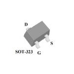
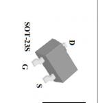
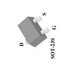
ORDERING INFORMATION Ordering Number | Package | Pin Assignment | Packing | Lead Free | Halogen Free | 1 | 2 | 3 | 2N60L-TF1-T | 2N60G-TF1-T | TO-220F1 | G | D | S | Tube | 2N60L-TF3-T | 2N60G-TF3-T | TO-220F | G | D | S | Tube | 2N60L-TM3-T | 2N60G-TM3-T | TO-251 | G | D | S | Tube |
Note: Pin Assignment: G: Gate D: Drain S: Source
MARKING
ABSOLUTE MAXIMUM RATINGS (TC = 25°С, unless otherwise specified)
PARAMETER | SYMBOL | RATINGS | UNIT | Drain-Source Voltage | VDSS | 600 | V | Gate-Source Voltage | VGSS | ± 30 | V | Drain Current | Continuous | ID | 2 | A | Pulsed (Note 2) | IDM | 4 | A | Avalanche Energy | Single Pulsed (Note 3) | EAS | 84 | mJ | Peak Diode Recovery dv/dt (Note 4) | dv/dt | 4.5 | V/ns | Power Dissipation | TO-220F/TO-220F1 | PD | 23 | W | TO-251 | 44 | W | Junction Temperature | TJ | +150 | °C | Storage Temperature | TSTG | -55 ~ +150 | °C |
Notes: 1. Absolute maximum ratings are those values beyond which
the device could be permanently damaged.
Absolute maximum ratings are stress ratings only and functional
device operation is not implied. Repetitive Rating: Pulse width limited by maximum junction
temperature. L = 84mH, IAS =1.4A, VDD = 50V, RG = 25 Ω Starting TJ = 25°C ISD ≤ 2.0A, di/dt ≤200A/μs, VDD ≤BVDSS, Starting TJ = 25°C
THERMAL DATA
PARAMETER | SYMBOL | RATINGS | UNIT | Junction to Ambient | TO-220F/TO-220F1 | θJA | 62.5 | °C/W | TO-251 | 100 | °C/W | Junction to Case | TO-220F/TO-220F1 | θJC | 5.5 | °C/W | TO-251 | 2.87 | °C/W |
ELECTRICAL CHARACTERISTICS (TJ = 25°С, unless otherwise specified)
PARAMETER | SYMBOL | TEST CONDITIONS | MIN | TYP | MAX | UNIT | OFF CHARACTERISTICS | Drain-Source Breakdown Voltage | BVDSS | VGS=0V, ID= 250μA | 600 | | | V | Drain-Source Leakage Current | IDSS | VDS=600V, VGS=0V | | | 1 | µA | Gate-Source Leakage Current | Forward | IGSS | VGS=30V, VDS=0V | | | 100 | nA | Reverse | VGS=-30V, VDS=0V | | | -100 | nA | ON CHARACTERISTICS | Gate Threshold Voltage | VGS(TH) | VDS=VGS, ID=250μA | 2.0 | | 4.0 | V | Static Drain-Source On-State Resistance | RDS(ON) | VGS=10V, ID=1.0A | | | 7.0 | Ω | DYNAMIC CHARACTERISTICS | Input Capacitance | CISS |
VGS=0V, VDS=25V, f=1.0 MHz | | 190 | | pF | Output Capacitance | COSS | | 28 | | pF | Reverse Transfer Capacitance | CRSS | | 2 | | pF | SWITCHING CHARACTERISTICS | Total Gate Charge (Note 1) | QG | VDS=200V, VGS=10V, ID=2.0A IG=1mA (Note 1, 2) | | 7 | | nC | Gateource Charge | QGS | | 2.9 | | nC | Gate-Drain Charge | QGD | | 1.9 | | nC | Turn-on Delay Time (Note 1) | tD(ON) |
VDS=300V, VGS=10V, ID=2.0A, RG=25Ω (Note 1, 2) | | 4 | | ns | Rise Time | tR | | 16 | | ns | Turn-off Delay Time | tD(OFF) | | 16 | | ns | Fall-Time | tF | | 19 | | ns | SOURCE- DRAIN DIODE RATINGS AND CHARACTERISTICS | Maximum Body-Diode Continuous Current | IS | | | | 2 | A | Maximum Body-Diode Pulsed Current | ISM | | | | 8 | A | Drain-Source Diode Forward Voltage (Note 1) | VSD | VGS=0V, IS=2.0A | | | 1.4 | V | Reverse Recovery Time (Note 1) | trr | VGS=0V, IS=2.0A,
dIF/dt=100A/µs (Note1) | | 232 | | ns | Reverse Recovery Charge | Qrr | | 1.1 | | µC |
Notes: 1. Pulse Test : Pulse width ≤ 300µs, Duty cycle ≤ 2%.
Essentially independent of operating temperature.
|