
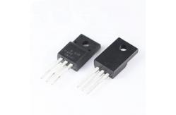
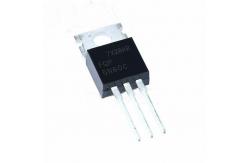
5N60 K-TCQ 5A 600V N-CHANNEL POWER MOSFET
|
|
5N60 K-TCQ 5A 600V N-CHANNEL POWER MOSFET
DESCRIPTIONThe UTC 5N60K-TCQ is a high voltage power MOSFET and is designed to have better characteristics, such as fast switching time, low gate charge, low on-state resistance and have a high rugged avalanche characteristics. This power MOSFET is usually used at high speed switching applications in power supplies, PWM motor controls, high efficient DC to DC converters and bridge circuits.
FEATURES RDS(ON) < 2.5Ω @ VGS =10V, ID = 2.5A * Fast Switching Capability * Avalanche Energy Specified * Improved dv/dt Capability, High Ruggedness
Application Load switching Hard switched and high frequency circuits Uninterruptible power supply
ORDERING INFORMATION
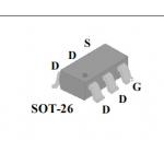
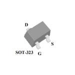
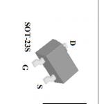
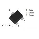
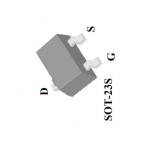
Note: Pin Assignment: G: Gate D: Drain S: Source
ABSOLUTE MAXIMUM RATINGS (TC = 25°С, unless otherwise specified)
Notes: 1. Absolute maximum ratings are those values beyond which the device could be permanently damaged. Absolute maximum ratings are stress ratings only and functional device operation is not implied. 4. Repetitive Rating: Pulse width limited by maximum junction temperature. 5. L = 84mH, IAS =1.4A, VDD = 50V, RG = 25 Ω Starting TJ = 25°C 6. ISD ≤ 2.0A, di/dt ≤200A/μs, VDD ≤BVDSS, Starting TJ = 25°C THERMAL DATA
ELECTRICAL CHARACTERISTICS (TJ = 25°С, unless otherwise specified)
Notes: 1. Pulse Test : Pulse width ≤ 300µs, Duty cycle ≤ 2%.
|
||||||||||||||||||||||||||||||||||||||||||||||||||||||||||||||||||||||||||||||||||||||||||||||||||||||||||||||||||||||||||||||||||||||||||||||||||||||||||||||||||||||||||||||||||||||||||||||||||||||||||||||||||||||||||||||||||||||||||||||||||||||||||||||||||||||||||||||||||||||||||||||||||||||||||||||||||||||||||||||||||||||||||||||||
| Product Tags: n channel mosfet transistor high voltage transistor | ||||||||||||||||||||||||||||||||||||||||||||||||||||||||||||||||||||||||||||||||||||||||||||||||||||||||||||||||||||||||||||||||||||||||||||||||||||||||||||||||||||||||||||||||||||||||||||||||||||||||||||||||||||||||||||||||||||||||||||||||||||||||||||||||||||||||||||||||||||||||||||||||||||||||||||||||||||||||||||||||||||||||||||||||
|
AP2602GY-HF FR4 board 2W 30A SOT-26 IC Voltage Regulator |
|
LED Inductor 0.35W 2.5A Mosfet Power Transistor AP1332GEU-HF |
|
Drive IC AP2308GEN SOT-23 0.69W 3.6A Mosfet Power Transistor |
|
AP2N1K2EN1 IC Chips SOT-723 0.15W 800mA MOSFET Transistor |
|
AP2322GN LOGIC ICS 0.833W 10A MOSFET Power Switch |
|
AP1334GEU-HF 0.35W 8A Mosfet Power Transistor New Condition |