
41 - 50 of 84
std notch sapphire substrate wafers
Selling leads
|
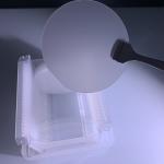
..., optoelectronic devices, semiconductor devices, and other fields. The high light transmittance and high hardness of sapphire wafers make them ...
2025-07-26 00:07:39
|
|
...> M-axis 2inch 3inch 4inch 6inch sapphire substrates wafers for GaN epitaxial growth;0.1mm/100um 2inch sapphire c-axis substrates TYPICAL CHOICES ...
2025-05-06 20:38:44
|
|
...> M-axis 2inch 3inch 4inch 6inch sapphire substrates wafers for GaN epitaxial growth;0.1mm/100um 2inch sapphire c-axis substrates TYPICAL CHOICES ...
2025-05-06 20:39:19
|
|
... The Kyropoulos process (KY process) for sapphire crystal growth is currently used by many companies in China to produce sapphire for the ...
2025-05-06 20:39:27
|
|
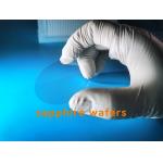
Ultra-thin 2inch sapphire DSP wafers thickness 100um 0.1mm Why Sapphire? One of the hardest materials available Superior IR & UV transmission compared ...
2025-05-06 20:38:38
|
|
... growth 430um SSP DSP About synthetic sapphire crystal Due to the less mismatched lattice and stable chemical and physical properties, sapphire...
2025-07-26 00:07:39
|
|
...11-20> R-axis M-axis 2inch 3inch 4inch 6inch sapphire substrates wafers for GaN epitaxial growth; TYPICAL CHOICES FOR PART ORIENTATION: Why ...
2025-05-06 20:38:38
|
|
...supplier of sapphire substrates for photoelectronic applications, including the high brightness LED market. The material is grown and orientated, ...
2025-07-26 00:07:39
|
|
...making them highly desirable for a wide range of applications. In fact, sapphire is one of the hardest and most scratch-resistant materials ...
2025-07-26 00:07:39
|
|
...sapphire substrate, including 2inch, 4inch and 6inch. It has clear aperture of over 90%, surface roughness of Ra less than 0.5nm, TTV of less than ...
2025-07-26 00:07:38
|