
1 - 10 of 45
sio2 thermal oxide silicon wafer
Selling leads

|
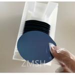
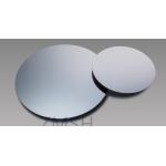
...Thermal Oxide (SiO2) On Silicon Wafers For Optical Communication System Generally, the oxide layer thickness of silicon wafers is mainly concentrat...
2025-08-01 00:08:35
|
|
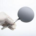
SiO2 wafer Thermal Oxide Laver Thickness 20um+5% MEMS Optical Communication System Product Description: The SIO2 silicon dioxide wafer serves as a ...
2025-05-06 20:45:05
|
|
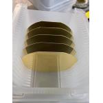
...silicon wafer DSP SiO2 wafers Silicon oxide wafer Polished Silicon Wafer High-purity (11N) 1-12 inch single- and double-polished Czochralski wafers ...
2025-05-06 20:44:47
|
|
... Polished Silicon Wafer High-purity (11N) 1-12 inch single- and double-polished Czochralski wafers Sizes 1" 2" 3" 4" 5" 6" 8" 12" and special size ...
2025-05-06 20:44:51
|
|
...silicon wafer DSP SiO2 wafers Silicon oxide wafer 1inch 2inch 10x10mm Scanning electron microscope silicon wafer small square piece SEM Polished ...
2025-05-06 20:44:47
|
|
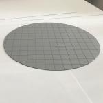
Electronic-Grade Silicon Wafers Ultra-High Purity Optoelectronic-Grade Abstract The high-purity silicon wafer we offer undergoes precision machining ...
2025-05-06 20:45:04
|
|
... Diameter 100 Mm +/- 0.5 Mm Oxygen Content 1.6 X 10^18 Atoms/cm3 Secondary Flat Length 18.0 +/- 2.0 Mm Thermal Expansion Coefficient 2.6·10-6°C -1 ...
2025-05-06 20:45:09
|
|
...Wafer Silicon Carbide Optoelectronic High-Power RF LEDS Description of 3C-N SiC Wafer: Compared to 4H-Sic, although the bandgap of 3C silicon ...
2025-05-06 20:41:48
|
|
... electrical and thermal properties. It is a high-performance semiconductor that is ideal for a wide variety of applications. In addition to its ...
2025-05-06 20:41:23
|
|
... for silicon carbide wafers. This type of wafer is preferred for its high carrier mobility, high thermal conductivity, and high chemical and ...
2025-05-06 20:41:30
|