
41 - 50 of 372
single crystal silicon wafers
Selling leads
|
2inch/3inch/4inch S/Fe/Zn doped InP Indium Phosphide Single Crystal Wafer Indium phosphide (InP) is an important compound semiconductor material with ...
2025-05-06 20:44:34
|
|
2inch InP wafers 3inch 4inch N/P TYPE InP Semiconductor Substrate Wafers Doped S+/ Zn+ /Fe + growth (modified VFG method) is used to pull a single ...
2025-05-06 20:44:36
|
|
8inch Dia200mm C-Plane Al2O3 99.999% Sapphire Single Crystal Wafer Carrier Substrate 1sp 2sp *, *::before, *::after {box-sizing: border-box; } * ...
2025-07-24 00:12:37
|
|
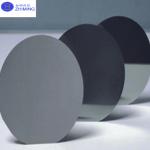
Silicon wafer Si wafer 8inch N type P type SSP DSP Prime grade Dummy grade Product Overview: 8-Inch Prime Grade Silicon Wafer Silicon wafers are the ...
2025-05-06 20:45:52
|
|
...wafer CZ 200mm Prime Grade Silicon Wafer , SSP,DSP P type,B dopant,for semiconducter matrial Product Introduction: 8-Inch (200mm) Prime Grade ...
2025-05-06 20:45:53
|
|
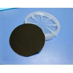
..., and an infrared light-emitting device with a wavelength of 2 to 14 μm can be fabricated. The AlGaSb superlattice structure material can also be ...
2025-05-06 20:44:36
|
|
... can be found in all types of electronic devices that improve the lives of people. Silicon comes second as the most common element in the universe; ...
2025-05-06 20:45:33
|
|
... Carrier wafers for SOS GaAs epitaxy About synthetic sapphire crystal The Kyropoulos process (KY process) for sapphire crystal growth is currently ...
2025-05-06 20:38:48
|
|
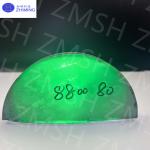
... material science applied to the jewelry industry. Derived from single-crystal silicon carbide (SiC), this gemstone exhibits a Mohs hardness of 9...
2025-05-06 20:47:08
|

|
... Silicon Wafers For Optical Communication System Generally, the oxide layer thickness of silicon wafers is mainly concentrated below 3um, and the ...
2025-07-24 00:12:37
|