
131 - 140 of 372
single crystal silicon wafers
Selling leads
|
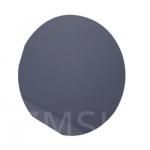
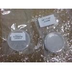
... Substrates. It has a crystal structure of silicon carbide where the silicon and carbon atoms are arranged in a cubic lattice with a diamond-like ...
2025-05-06 20:41:43
|
|
... containing silicon and carbon with chemical formula SiC. SiC is used in semiconductor electronics devices that operate at high temperatures or ...
2025-05-06 20:40:48
|
|
... containing silicon and carbon with chemical formula SiC. SiC is used in semiconductor electronics devices that operate at high temperatures or ...
2025-05-06 20:40:41
|
|
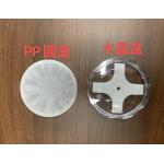
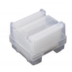
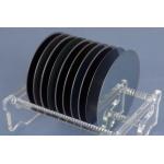
...Single Wafer Carrier, Single Wafer Sample Box for Silicon, Sapphire, SiC Substrate Cleanroom Class 100 Grade 1 inch Style Single Wafer Carrier ...
2025-05-06 20:47:34
|
|
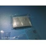
... to a silicon carbide (SiC) wafer with a 12-inch diameter (approximately 300mm), a size standard used in the semiconductor industry for the mass ...
2025-05-06 20:41:54
|
|
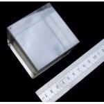
...wafer carrier container cassette box for wafer shipment factory price 6" Diameter Single Wafer Carrier Box Wafer Box Customized Processing Square ...
2025-05-06 20:47:35
|
|
...wafer 1-5um AlN template 8inch 6inch AlGaN/GaN HEMT-on-HR Si Epiwafer GaN-on-Si Epiwafer for Micro-LED for RF application GaN Wafer Characteristic ...
2025-05-06 20:44:19
|
|
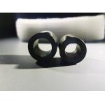
...crystal rod Lens diameter2mm 10mm length High Precision 1mm 2mm 3mm 4mm 5mm 6mm 24mm Etc Silicon Carbide Ceramic Ball For Bearing Sic Beads ...
2025-07-30 00:08:00
|
|
...: The ion implantation machine is used to drive high-energy He ions from the upper surface of lithium niobate crystal. When He ions with specific ...
2025-05-06 20:44:59
|
|
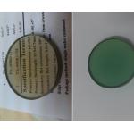
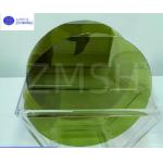
...crystals crystal substrate TeO2 wafer TeO2 Crystal & Q Switch TeO2 is an excellent ascousto-optic (AO) crystal with high AO figure of merit, ...
2025-05-06 20:40:28
|