
171 - 180 of 369
single crystal semiconductor substrate
Selling leads
|
...Material Sapphire(Al2O3) Density(20°C) Kg/M3 3.98×10³ Crystal Structure Hexagonal Crystal Lattice Constant A=4.785Å C=12.991 Å Mohs Hardness 9 ...
2025-05-06 20:39:16
|
|
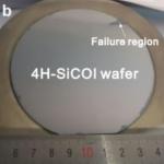
...500–600 nm, depending on specific applications) onto a silicon dioxide (SiO₂) substrate. SiC is renowned for its exceptional thermal conductivity, ...
2025-05-27 17:33:30
|
|
...PART ORIENTATION: Why Sapphire? Zero Degree: The direction of view is parallel to the optical axis of the crystal 90 Degree: The direction of view ...
2025-05-06 20:38:55
|
|
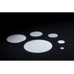
... Sapphire single crystal watch glass case/ Sapphire optical glass for watch lens Sapphire Glass Sapphire optical windows are ideal for applications ...
2025-05-27 17:33:20
|
|
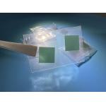
... For seed growth 6H-N/6H-Semi 4H HPSI 5*10mmt 10x10mmt 5*5mm polished Silicon Carbide sic substrate chips Wafer About Silicon Carbide (SiC)Crystal ...
2025-07-29 00:07:53
|
|
... For seed growth 6H-N/6H-Semi 4H HPSI 5*10mmt 10x10mmt 5*5mm polished Silicon Carbide sic substrate chips Wafer About Silicon Carbide (SiC)Crystal ...
2025-07-29 00:07:53
|
|
Product Overview TGV (Through Glass Via) technology, also known as glass through-hole technology, is a vertical electrical interconnection technique ...
2025-07-29 00:07:53
|
|
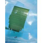
...Monocrystal KY Method LED Semiconductor 1. Abstract Our Sapphire Material 99.999% Al2O3 Monocrystal, produced using the KY (Kyropoulos) method, is ...
2025-05-06 20:40:05
|
|
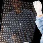
... 4inch 6inch sapphire substrates wafers for GaN epitaxial growth;0.1mm/100um 2inch sapphire c-axis substrates TYPICAL CHOICES FOR PART ORIENTATION: ...
2025-05-06 20:38:52
|
|
Si wafer 4inch Polished CZ Dopant Arsenic(As) Boron(B) Phosphorus(Ph) (100) Semiconductor Describe of Si Wafer: A Silicon wafer is a very thin round ...
2025-05-06 20:45:29
|