
121 - 130 of 307
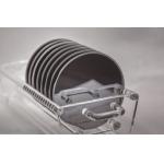
single crystal aln substrate
Selling leads
|
2-6 inch Gallium phosphide (GaP) crystals crystal substrate,GaP wafer ZMKJ can provides 2inch GaP wafer – gallium Phosphide which are grown by LEC...
2025-05-06 20:44:33
|
|
...: The ion implantation machine is used to drive high-energy He ions from the upper surface of lithium niobate crystal. When He ions with specific ...
2025-05-06 20:44:59
|
|
...substrates template,GaN wafer for LeD,semiconducting Gallium Nitride Wafer for ld,GaN template, mocvd GaN Wafer,Free-standing GaN Substrates by ...
2025-05-06 20:44:29
|
|
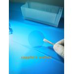
...substrates wafers for GaN epitaxial growth;0.1mm/100um 2inch sapphire c-axis substrates TYPICAL CHOICES FOR PART ORIENTATION: Why Sapphire? Zero ...
2025-05-06 20:38:43
|

|
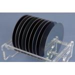
...crystal Dia50.8mm M-axis 2Inch Sapphire Wafers For epitaxial Thickness 500um Double side polished DSP Special Orientation SSP/ DSP A-axis R-axis M...
2025-05-06 20:38:51
|
|
...Substrate Lithium niobate (LiNbO3) crystal is an important photoelectric material, and is widely used in integrated optics, nonlinear optics, ...
2025-05-06 20:44:57
|
|
Product Description: Ce:YAG single crystal is a high-performance scintillation crystal with a light emission center wavelength of 550nm. It offers a ...
2025-05-06 20:46:20
|
|
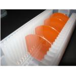
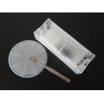
2inch 50.8mm sapphire DSP wafers thickness 430+/-15um 2inch 430um Ultra Thin sapphire wafers 0.43mm Thickness C-plane/M-plane/A-plane DSP/SSP Sapphire ...
2025-05-06 20:39:14
|
|
... Degree: The direction of view is parallel to the optical axis of the crystal 90 Degree: The direction of view is perpendicular to the optical axis ...
2025-05-06 20:38:37
|
|
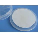
...Substrate wafers thickness 1.5mm C-a 4inch dia100mm prime grade DSP/SSP 0.5mm thickness Al2O3 Sapphire wafers TYPICAL CHOICES FOR PART ORIENTATION: ...
2025-05-06 20:38:56
|