
11 - 20 of 123
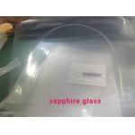
optoelectronics sapphire wafer
Selling leads
|
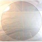
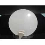
... dia150mm C-plane Sapphire SSP/DSP wafers with 650um/1000um Thicknessdiameter300mm 12inch Al2O3 Sapphire wafers carrier with notch SSP DSP 1.0mm C ...
2025-05-06 20:40:26
|

|
... The Kyropoulos process (KY process) for sapphire crystal growth is currently used by many companies in China to produce sapphire for the ...
2025-05-06 20:39:27
|
|
... 12inch diameter 300mm with notch DSP Sapphire Substrate wafers thickness 1.5mm C-a 4inch dia100mm prime grade DSP/SSP 0.5mm thickness Al2O3 ...
2025-05-06 20:38:56
|
|
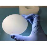
... quality for semiconductor applications. Known for its superior optical transparency, outstanding mechanical strength, and excellent thermal ...
2025-05-06 20:40:12
|
|
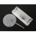
... resistant Highly chemical resistant Maximum temperature rating of almost 2000C The Detail for 2inch C-axis wafers Size: 2 inch DSP-0.1-C-Sapphire ...
2025-05-06 20:38:38
|
|
...material in nature, after diamond. Sapphire has good light transmittance, high strength, collision resistance, wear resistance, corrosion ...
2025-05-06 20:39:26
|
|
... Carrier wafers for SOS GaAs epitaxy About synthetic sapphire crystal The Kyropoulos process (KY process) for sapphire crystal growth is currently ...
2025-05-06 20:38:48
|
|
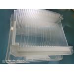
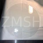
...sapphire substrate, including 2inch, 4inch and 6inch. It has clear aperture of over 90%, surface roughness of Ra less than 0.5nm, TTV of less than ...
2025-08-01 00:08:35
|
|
Sapphire wafer 8inch Diameter 200mm C Plane A Plane KY EFG Double Slide Polished Product Description: In 1992, Japanese engineer Shuji Nakamura ...
2025-05-06 20:39:56
|
|
... diameter 300mm with notch DSP Sapphire Substrate wafers thickness 1.5mm C-a Diameter 156mm 200mm 8inch double side polished Sapphire Substrate for ...
2025-05-06 20:38:54
|