
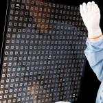
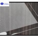
4inch 101.6mm Sapphire Wafer Substrate Carrier Single Side Polished Single Crystal Al2O3
|


|
4inch 101.6mm Sapphire Wafer Substrate Carrier Single Side Polished Single Crystal Al2O3 About synthetic sapphire crystalSapphire is a single crystal of alumina and is the second-hardest material in nature, after diamond. Sapphire has good light transmittance, high strength, collision resistance, wear resistance, corrosion resistance, and high temperature and high-pressure resistance, biocompatibility is an ideal substrate material for the production of semiconductor optoelectronic devices, the electrical properties of sapphire make it become the substrate material for the production of the white and blue LED. Our company's long-term production thickness ≧0.1mm, and its shape size ≧Φ2" high precision sapphire wafer. In addition to the conventional Φ2 ", Φ4 ", Φ6 ", Φ8 ", Φ10 ", Φ12 " and other sizes can be customized, please contact our sales staff. The sapphire (Al₂O) ₃ substrate is a kind of material for LED chips. Due to its high stability, sapphire ₃ is suitable for high-temperature growth. Finally, sapphire is mechanically strong and easy to handle and clean. Therefore, sapphire is generally used as a substrate for most processes. Sapphire Properties
Synthetic sapphire is a transparent single crystal 99.99% pure Al2O3 that exhibits a
unique combination of physical, chemical, electrical and optical
properties: high thermal conductivity, high strength, scratch
resistance, hardness (9 on the Mohs scale), transparent in a wide
range of wavelength, chemical inertness. It drives the development of new markets like general lighting, backside lighting in TV-sets, displays, consumer appliances, aerospace and defense, and other applications Specifications of 4inch sapphire wafer substrate carrier
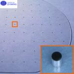
The material is grown and orientated, and substrates are fabricated and polished to an extremely smooth damage free Epi-Ready surface on one or both sides of the wafer. A variety of wafer orientations and sizes up to 6" in diameter are available. A-Plane sapphire substrates - are usually used for hybrid microelectronic applications requiring a uniform dielectric constant and highly insulating characteristics. C-Plane substrates - tend to be used for all-V and ll-Vl compounds, such as GaN, for bright blue and green LED and laser diodes. R-Plane substrates - these are preferred for the hetero-epitaxial deposition of silicon used in microelectronic IC applications.
101.6mm 4inch Sapphire wafer sapphire DetailsOther related sapphire productsGaN wafer quartz plate sapphire cover glass sapphire customized wafer sapphire rod lens colored sapphire ruby sic wafers |
||||||||||||||||||||||||||||||||||||||||||||||||||||||||||||||||||||||||||||||||||||||||||||||||||||||||||||||||||||
| Product Tags: 4inch Sapphire Wafer Substrate Carrier Single Crystal Al2O3 Sapphire Substrate Single Side Polished Substrate Carrier | ||||||||||||||||||||||||||||||||||||||||||||||||||||||||||||||||||||||||||||||||||||||||||||||||||||||||||||||||||||
|
TGV Glass Substrate Through-hole Coating Semiconductor Packaging JGS1 JGS2 |
|
Royal Blue Sapphire Raw Gemstone Synthetic Colored For Durable Exquisite Jewelry & Watch Case |
|
Sapphire Wafer Monocrystal Al2O3 DSP SSP 2inch 4inch 6inch 8inch 12inch A plane C plane |
|
Sapphire wafer 2inch C-plane(0001) DSP SSP 99,999% Monocrystalline Al2O3 LEDS Semiconductor |
|
Through Glass Vias (TGV) For JGS1 JGS2 Sapphire Corning Glass For Sensors Manufacturing And Packaging |
|
Through Glass Vias (TGV) JGS1 JGS2 Sapphire BF33 Quartz Customizable Dimensions Thickness Can Low As 100 Μm |