
371 - 380 of 395
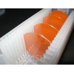
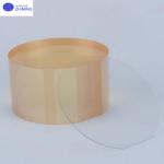
high transmittance sapphire substrate
Selling leads

|
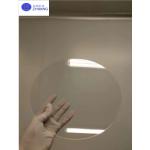
SapphiLarge Thickness Thermal Oxide (SiO2) On Silicon Wafers For Optical Communication System Generally, the oxide layer thickness of silicon wafers ...
2025-07-30 00:08:00
|
|
GaP Wafer, Gallium Phosphide single crystal Orientation (111)A 0°±0.2 Solar Cells Product Description: Gallium Phosphide GaP, an important semiconduct...
2025-05-06 20:45:06
|
|
Epi ready 4inch InP wafers N-type p-type EPF<1000cm^2 with the thickness of 325um±50um Product abstract Our product, the "High-Purity Indium Phosphide ...
2025-05-06 20:45:10
|
|
Fused Silica wafer JGS1 JGS2 BF33 8inch 12inch thickeness 750um±25um Ra ≤ 0.5nm TTV ≤ 10um Fused Silica wafer JGS1 JGS2 BF33 8inch 12inch‘s summary ...
2025-05-06 20:45:40
|
|
ZnTe: ZnTe wafer, ZnTe crystal Type N, Type P, Custom Sizes and Specifications Available Abstract of ZnTe Zinc telluride (ZnTe) is a direct bandgap ...
2025-05-06 20:45:56
|
|
LiTaO3 Wafer Lithium Tantalate Electro-Optic Nonlinear Optical Piezoelectric Customization Introduce of LiTaO3 Wafer Lithium tantalate is an excellent ...
2025-06-23 17:12:59
|
|
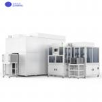
...machine combines one ceramic disc cleaner with dual ceramic disc mounters, designed for high-efficiency cleaning and wafer waxing in sapphire and ...
2025-05-13 05:30:32
|
|
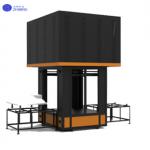
...Introduction This series of calcination annealing furnaces is widely used for annealing sapphire crystal rods and wafers, sintering special ...
2025-05-13 05:30:23
|
|
|
...Introduction This series of calcination annealing furnaces is widely used for annealing sapphire crystal rods and wafers, sintering special ...
2025-05-13 05:30:00
|
|
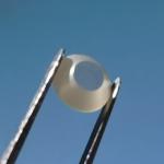
...demanding environments requiring high thermal stability, exceptional hardness, and excellent infrared transmission. Compared with traditional glass ...
2025-06-24 07:30:26
|