
211 - 220 of 225
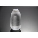
doped ruby sapphire crystal
Selling leads
|
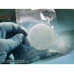
2inch InP wafers 3inch 4inch N/P TYPE InP Semiconductor Substrate Wafers Doped S+/ Zn+ /Fe + growth (modified VFG method) is used to pull a single ...
2025-05-06 20:44:37
|
|
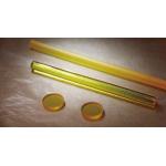
Nd,Ce:YAG Laser Crystal 1inch 2inch 10x10mmt YAG Plates Yttrium Aluminum Garnet Wafer Product Type: Nd,Ce: YAG(neodymium-doped and cerium Yttrium ...
2025-07-24 00:12:37
|
|
...Sapphire Epi-wafer 1-5um AlN template 8inch 6inch AlGaN/GaN HEMT-on-HR Si Epiwafer GaN-on-Si Epiwafer for Micro-LED for RF application GaN Wafer ...
2025-05-06 20:44:19
|
|
VFG metod N-type 2inch/3inch,4inch ,6inch dia150mm GaAs Gallium Arsenide Wafers N-type Semi-insulating type for Microelectronics, --------------------...
2025-05-06 20:44:43
|
|
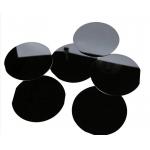
...crystals substrate wafer for laser device Product Type: Terbium gallium garnet (TGG) crystal substrateProduct Description:TGG crystal with a large ...
2025-05-06 20:40:28
|
|
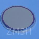
...crystals substrate wafer for laser device Product Type: Yttrium aluminum garnet (YAG) is an isotropic crystal with cubic symmetry. It has excellent ...
2025-07-24 00:12:37
|
|
...crystal silicon carbide wafer with a 4H crystal structure that is doped with acceptor impurities, making it a P-type semiconductor material. 6H P...
2025-05-06 20:41:39
|
|
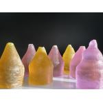
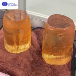
...doped Gadolinium Gallium Garnet) is a synthetic rare-earth optical crystal that exhibits a distinctive brown hue due to controlled doping ...
2025-05-27 17:33:45
|
|
...150mm silicon carbide single crystal (sic) substrates wafersS/ High purity un-doped 4H-semi resistivity>1E7 3inch 4inch 0.35mm sic wafers About ...
2025-05-06 20:40:51
|
|
.../3inch /4inch /6inch S-C-N Type/ semi-insulation /Si-doped Gallium arsenide GaAs Wafer Product Description Our 2’’ to 6’’ semi-conducting & semi...
2025-05-06 20:44:32
|