
51 - 60 of 123
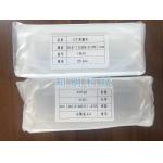
bf33 sapphire substrate
Selling leads
|
...11-20> R-axis M-axis 2inch 3inch 4inch 6inch sapphire substrates wafers for GaN epitaxial growth; TYPICAL CHOICES FOR PART ORIENTATION: Why ...
2025-05-06 20:38:38
|
|
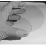
Sapphire wafer 8inch Diameter 200mm C Plane A Plane KY EFG Double Slide Polished Product Description: In 1992, Japanese engineer Shuji Nakamura ...
2025-05-06 20:39:56
|
|
...Sapphire Window Substrates Wafer DSP Notch High Precision 8inch/6inch/5inch/ 2inch /3inch 4inch /5inch C-axis/ a-axis/ r-axis/ m-axis 6"/6inch ...
2025-05-06 20:39:17
|

|
... The Kyropoulos process (KY process) for sapphire crystal growth is currently used by many companies in China to produce sapphire for the ...
2025-05-06 20:39:27
|
|
2inch 4inch 4" Sapphire based GaN templates GaN film on sapphire substrate Properties of GaN Chemical properties of GaN 1) At room temperature, GaN is ...
2025-05-06 20:39:23
|

|
...making them highly desirable for a wide range of applications. In fact, sapphire is one of the hardest and most scratch-resistant materials ...
2025-08-01 00:08:35
|

|
2inch 50.8mm C Miscut A 4 Degree Sapphire Wafers Thickness 0.175mm/0.3mm/0.4mm/0.5mm Dsp 2 Inch C Plane Polished Sapphire Wafers Crystal Substrates ...
2025-08-01 00:08:35
|
|
Ultra-thin 2inch sapphire DSP wafers thickness 100um 0.1mm Why Sapphire? One of the hardest materials available Superior IR & UV transmission compared ...
2025-05-06 20:38:38
|
|
2inch 4iinch 6Inch Sapphire based AlN templates AlN film on sapphire substrate sapphire window sapphire wafer Applications of AlN template Silicon...
2025-05-06 20:44:39
|
|
6 Inch 153mm 156mm 159mm Thickness 350um 0.5mmt Sapphire Carrier Substrate Wafer SSP DSP Product Description: Sapphire bonding sheet is used for ...
2025-08-01 00:08:35
|