
11 - 20 of 175
5g saw semiconductor substrate
Selling leads
|
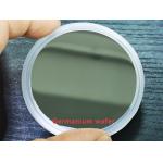
...substrate Ge window for infrared Co2 lasers Ge Material Introduce Among optical materials, germanium materials are increasingly widely used in ...
2025-05-06 20:44:48
|
|
2INCH dia50.8mm Ga doped Ge substrate 4inch N-type 500um Ge wafers Ge wafer for microelectronic application N type, Sb doped Ge wafer N type,undoped ...
2025-05-06 20:44:46
|
|
VGF 2inch 4inch 6inch n-type prime grade GaAs wafer for epitaxial growth GaAs wafer (Gallium Arsenide) is an advantageous alternative to silicon that ...
2025-05-06 20:44:45
|
|
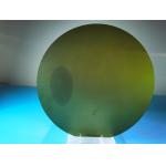
2inch 4inch 4" Sapphire based GaN templates GaN film on sapphire substrate Properties of GaN Chemical properties of GaN 1) At room temperature, GaN is ...
2025-05-06 20:44:40
|
|
2inch N-type single side polished Ge wafers Germanium substrate Ge window for infrared Co2 lasers Diameter:25.4mm Thickness:0.325mm Shanghai Famous ...
2025-05-06 20:44:50
|
|
VFG metod N-type 2inch/3inch,4inch ,6inch dia150mm GaAs Gallium Arsenide Wafers N-type Semi-insulating type for Microelectronics, --------------------...
2025-05-06 20:44:31
|
|
2inch/3inch/4inch S/Fe/Zn doped InP Indium Phosphide Single Crystal Wafer Indium phosphide (InP) is an important compound semiconductor material with ...
2025-05-06 20:44:34
|
|
VFG metod N-type 2inch/3inch,4inch ,6inch dia150mm GaAs Gallium Arsenide Wafers N-type Semi-insulating type for Microelectronics, --------------------...
2025-05-06 20:44:43
|
|
...Substrate/Wafers (150mm, 200mm) Silicon Carbide Ceramic Excellent CorrosionSingle crystal single side polished silicon wafer sic wafer polishing ...
2025-05-06 20:41:07
|
|
2inch 4inch 4" 2'' Sapphire based GaN templates GaN film on the sapphire substrate GaN-On-Sapphire GaN wafers GaN substrates GaN windows Properties of ...
2025-05-06 20:44:20
|