
261 - 270 of 313
technical ceramic plunger parts
Selling leads

|
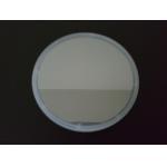
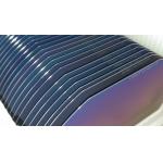
Sapphire Wafer, making blue LED , high Tc superconductor and microwave IC Semiconductor Wafer Inc. provides single crystal sapphire wafer to ...
2024-12-09 19:40:24
|
|
GaAs Based Epi Wafer We provides MBE / MOCVD epitaxial growth of custom structure on GaAs substrate for microelectronics , optoelectronics and RF ...
2024-12-09 19:40:24
|
|
InAs wafer ( Indium Arsenide ) We provides InAs wafer ( Indium Arsenide ) to optoelectronics industry in diameter up to 2 inch . InAs crystal is a ...
2024-12-09 19:40:24
|
|
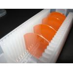
Single Crystal GaP Wafer ( Gallium Phosphide ),widely used as red , yellow , and green LED ( light-emitting diodes ) We provides high quality single ...
2024-12-09 19:40:24
|
|
Single crystal and polycrystalline GaAs wafer ( Gallium Arsenide ) for making LD , LED , microwave circuit, solar cell We provides both single crystal ...
2024-12-09 19:40:24
|
|
Ge wafer to micro-electronics and opto-electronics industry in diameter range from 2 inch to 4 inch We are a worldwide supplier of single crystal Ge ...
2024-12-09 19:40:24
|

|
Thermal Oxide Wafer, higher uniformity, and higher dielectric strength , excellent dielectric layer as an insulator Thermal oxide or silicon dioxide ...
2024-12-09 19:40:24
|

|
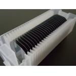
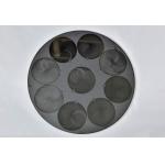
SiC Micro-Reaction Plate SiC micro-reaction plates are formed by isostatic pressing and sintering at high temperature.According to the special needs ...
2024-12-09 19:40:24
|
|
SiC ICP Tray Silicon carbide ICP tray is formed by isostatic pressing process and sintering at high temperature. The outer diameter, thickness, number ...
2024-12-09 19:40:24
|
|
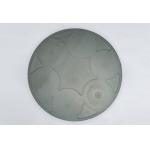
SiC PVD Tray Silicon carbide PVD tray is formed by isostatic pressing process and sintering at high temperature. The outer diameter, thickness, number ...
2024-12-09 19:40:24
|