
171 - 180 of 392
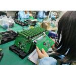
double sided smt pcb assembly
Selling leads

|
... Assembly , Through-Hole Assembly ,Mixed Assembly,Rigid Flex PCB Assembly services . etc. Basic Information Model NO. PCBA Condition New MOQ 1 PCs ...
2026-05-23 00:17:19
|

|
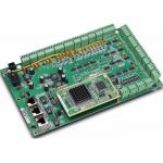
...PCB Assembly Our Electronics Printed Circuit Board Assembly complete solutions include : Surface Mount Technology (SMT Assembly) Through-Hole ...
2026-05-23 00:17:19
|
|
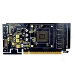
...ough holes on a printed circuit board (PCB) by the pins of the component by an automatic insert mount machine or manual soldering. As to soldering ...
2024-12-09 20:47:07
|
|
|
...ough holes on a printed circuit board (PCB) by the pins of the component by an automatic insert mount machine or manual soldering. As to soldering ...
2026-05-23 00:17:19
|

|
...PCB Assembly Lead-Free PCB Assembly Introduction PCBA is the abbreviation of Printed Circuit Board Assembly in English, that is to say, PCB blank ...
2024-12-09 20:26:12
|
|
...blank board goes through SMT loading, or the entire process of DIP plug-in, referred to as PCBA, and the standard way of writing in Europe and ...
2024-12-09 20:26:12
|
|
|
...PCB Assembly Lead-Free PCB Assembly Introduction PCBA is the abbreviation of Printed Circuit Board Assembly in English, that is to say, PCB blank ...
2026-05-23 00:17:19
|
|
|
...blank board goes through SMT loading, or the entire process of DIP plug-in, referred to as PCBA, and the standard way of writing in Europe and ...
2026-05-23 00:17:19
|
|
... DIP Multilayer Double Side Lead Free PCB Assembly Lead Free PCB Assembly Introduction 15 years of custom PCB and PCBA manufacturer, PCB electronic ...
2024-12-09 20:40:49
|
|
|
... DIP Multilayer Double Side Lead Free PCB Assembly Lead Free PCB Assembly Introduction 15 years of custom PCB and PCBA manufacturer, PCB electronic ...
2026-05-23 00:17:19
|