
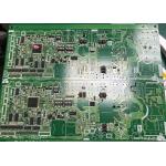
HASL FR4 Green Ink 6 Layers Lead Free Electronics PCB Assembly
|


HASL FR4 Green Ink 6 Layers Electronics PCBA Lead-Free PCB Assembly
Lead-Free PCB Assembly Introduction
PCBA is the abbreviation of Printed Circuit Board Assembly in English, that is to say, PCB blank board goes through SMT loading, or the entire process of DIP plug-in, referred to as PCBA, and the standard way of writing in Europe and America is PCB'A. Beijing Haina Lean is a professional PCB & PCB'A manufacturer which was established in 2006 and focus on circuit board design and layout, 2-46 layers PCB manufacturing, professional FPC production, electronic components purchasing, SMT professional processing, Soldering and Assembly, especially sample, small and bulk orders.
PCBA CAPABILITIES
PCB assembly process
Drilling---Exposure---Plating---Etaching & Stripping---Punching---Electrical Testing---SMT--Wave Soldering---Assembling---ICT--Function Testing---Temperature & Humidity Testing
Lead-Free PCB Assembly Delivery Time
Lead-Free PCB Assembly Application Field
Printed circuit boards And PCB Assembly are mainly used for many communication industry ,Aprospace ,Auto Industry ,Communication,Indutrial Control ,Medical device ,Smart Home,consumer electronics ,automotive electronics , audio and video, optoelectronics, robotics, hydroelectric power, aerospace, education, power supply, printer ,Auto Industry ,Smart Home.etc.
Workshop
Common packaging
1.PCB: Vacuum packaging with carton box
Company Brief Information
Haina lean Electronics Co., Ltd is a one-stop EMS supplier integrating PCB design, PCB manufacturing, Component sourcing and PCB assembly. Here is strong component supply chain and procceurement team. Prototype and mass production are available. Competitive price is for high-quality and services. Exported to worldwide customer in US, Europe, Canada.
|
||||||||||||||||||||||||||||||||||||||||||||||||||||||||||||||||||||||||||||||||||||||||||||||||||||||||||||||||||||||||||||||||||||||||||||||||||||||
| Product Tags: Green Lead Free PCBA 3OZ Electronics PCB Assembly 6 Layers Electronics PCB Assembly | ||||||||||||||||||||||||||||||||||||||||||||||||||||||||||||||||||||||||||||||||||||||||||||||||||||||||||||||||||||||||||||||||||||||||||||||||||||||
|
100% Lead Free Prototype Pcb Assembly Solder Paste Multi-Layer |

|
4 Layers Rohs Lead Free Pcb Assembly Compliance Surface Mount Technology |

|
6 Layers Hdi 1oz Medical Pcb Assembly Bga 0.18mm 3/3 Mil Trace |

|
Enig Finger Gold Fr 4 Pcb Assembly 8 Layer Hasl |

|
Multilayer Lead Free Pcb Assembly Buried Blind Hole Plate Dip Hasl |
|
1oz Rigid Cem-1 Turnkey Pcb Assembly Hasl One Stop Service |