
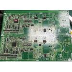
Multilayer Lead Free Pcb Assembly Buried Blind Hole Plate Dip Hasl
|


Multilayer Buried Blind Hole Plate DIP HASL Lead Free PCB Assembly
Lead Free PCB Assembly Introduction
Lead is the most comprehensive substance because it plays a fundamental & key role in electronic plating. Components used in lead-free PCB assembly should meet the requirements of lead-free compliance to ensure the reliability and suitability of final products. With more than 15 years' experience, Haina Lean Technology has maintained long-term cooperation relationship between renowned component manufacturers and distributors around the world, and we can purchase high quality lead-free components for our customers and care the environmental concerns.
PCBA CAPABILITIES
PCB assembly process
Drilling---Exposure---Plating---Etaching & Stripping---Punching---Electrical Testing---SMT--Wave Soldering---Assembling---ICT--Function Testing---Temperature & Humidity Testing
Lead-Free PCB Assembly Delivery Time
Lead-Free PCB Assembly Application Field
Printed circuit boards And PCB Assembly are mainly used for many communication industry ,Aprospace ,Auto Industry ,Communication,Indutrial Control ,Medical device ,Smart Home,consumer electronics ,automotive electronics , audio and video, optoelectronics, robotics, hydroelectric power, aerospace, education, power supply, printer ,Auto Industry ,Smart Home.etc.
Workshop
Common packaging
1.PCB: Vacuum packaging with carton box
BEIJING HAINA LEAN TECHNOLOGY CO., LTD offers full serial electronics production services for worldwide customers: everything from the initial idea to the start of mass production based on client's individual needs and technical requirements. |
|||||||||||||||||||||||||||||||||||||||||||||||||||||||||||||||||||||||||||||||||||||||||||
| Product Tags: multilayer lead free pcb assembly buried lead free pcb assembly blind hole lead free pcba |
|
100% Lead Free Prototype Pcb Assembly Solder Paste Multi-Layer |

|
4 Layers Rohs Lead Free Pcb Assembly Compliance Surface Mount Technology |

|
6 Layers Hdi 1oz Medical Pcb Assembly Bga 0.18mm 3/3 Mil Trace |

|
Enig Finger Gold Fr 4 Pcb Assembly 8 Layer Hasl |

|
Multilayer Lead Free Pcb Assembly Buried Blind Hole Plate Dip Hasl |
|
1oz Rigid Cem-1 Turnkey Pcb Assembly Hasl One Stop Service |