
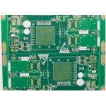
1.6mm Multi-Layers Hdi Pcb Board 53.7*56mm Size
|


ENIG 2.0mm Multi-layers 1oz HDI PCB Printed Circuit BoardHDI PCB Board Introduction
High Density Interconnection,shorted as (HDI) PCB, is a kind of (technology) for the production of printed circuit boards. It is a circuit board with relatively high circuit distribution density using micro blind via and buried via technology. Adopting the structure of Stripline and Microstrip, multi-layering becomes a necessary design. In order to reduce the quality problem of signal transmission, insulating materials with low dielectric constant and low attenuation rate are used. To meet the miniaturization and arraying of electronic components, the density of circuit boards is constantly increasing to meet the demand.
PCB CAPABILITIES
The types of HDI PCB
HDI (High Density Interconnection) circuit boards usually include laser blind vias and mechanical blind vias; general through buried vias, blind vias, stacked vias, staggered vias, cross blind buried, through vias, blind via filling plating, fine line small gaps, The technology of realizing the conduction between the inner and outer layers by processes such as micro-holes in the disk, usually the diameter of the blind buried is not more than 6 mils.
Work flow for HDI
Board Cut - Inner Wet film -DES - AOI - Brown Oxido - Outer Layer Press - Out Layer Lamination - X-RAY & Rounting - Copper reduce & brown oxide - Laser Drilling - Drilling - Desmear PTH - Panel plating - Outer Layer dry film - Etching - AOI- Impedance Testing - S/M Pluged hole - Solder Mask - Component Mark - Impedance testing - Immersion Gold -V-cut - Routing - Electrical Test - FQC - FQA -Package -Shipment
Similar products PCBA goods
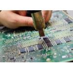
Workshop
Common packaging
1.PCB: Vacuum packaging with carton box
Our advantage
1.Service value Independent quotation system to quickly serve the market 2.PCB manufacturing High-tech PCB and PCB assembly production line 3.Material purchasing A team of experienced electronic component procurement engineers 4.SMT post soldering Dust-free workshop, high-end SMT patch processing
|
||||||||||||||||||||||||||||||||||||||||||||||||||||||||||||||||||||||||||
| Product Tags: 1.6mm hdi pcb board 53.7*56mm hdi pcb board hdi high density interconnect | ||||||||||||||||||||||||||||||||||||||||||||||||||||||||||||||||||||||||||
|
Blind Buried Vias Hole High Density PCB HDI PCB Stackup |

|
Fr-4 6 Layer Hdi Pcb Manufacturing Service For Communications |

|
1.6mm Multi-Layers Hdi Pcb Board 53.7*56mm Size |
|
Green High End Hdi Pcb Board For Automotive Electronics |

|
94v0 1oz Enig Hdi Pcb Board 4layer Oem Fabricating |

|
Buried Vias Enig Oem Pcb Board Multi-Layering 1oz Hdi |